
Stack-up electronic part and manufacturing method thereof

A technology of electronic components and manufacturing methods, which is applied to transformer/inductor components, inductor/transformer/magnet manufacturing, electrical components, etc., and can solve problems such as increased equivalent series resistance, increased AC resistance, and reduced Q characteristics. , to reduce the AC resistance and increase the magnetic flux

Active Publication Date: 2017-03-22
SAMSUNG ELECTRO MECHANICS CO LTD
View PDF6 Cites 3 Cited by
  • Summary
  • Abstract
  • Description
  • Claims
  • Application Information

AI Technical Summary

Problems solved by technology

[0009] The skin effect (Skin Effect) and parasitic effect (Parasitic Effect) caused by the increase of AC frequency lead to the increase of AC resistance and the increase of equivalent series resistance
[0010] That is, as the interlayer distance of the coil and the distance between the coil and the external electrode become smaller, the equivalent series resistance becomes larger due to the proximity effect and the rise of parasitic capacitance, and becomes larger as the frequency becomes higher due to the skin effect large, resulting in reduced Q characteristics

Method used


Image

  • Stack-up electronic part and manufacturing method thereof
  • Stack-up electronic part and manufacturing method thereof
  • Stack-up electronic part and manufacturing method thereof

Examples


Embodiment Construction

[0031] Hereinafter, embodiments of the present invention will be described with reference to specific embodiments and drawings. However, the embodiments of the present invention can be modified into various other forms, and the scope of the present invention is not limited to the embodiments described below. In addition, the epic form of the present invention is provided to more completely explain the present invention to those skilled in the art with average knowledge. Therefore, for clearer description, the shapes and sizes of elements in the drawings may be exaggerated, and elements denoted by the same symbols in the drawings are all the same elements.

[0032] In addition, in order to explain the present invention more clearly, in the drawings, parts irrelevant to the description are omitted, and the thicknesses are shown enlarged in order to clearly show a plurality of layers and regions, and configurations with the same functions within the same concept Components are d...


PUM


Abstract

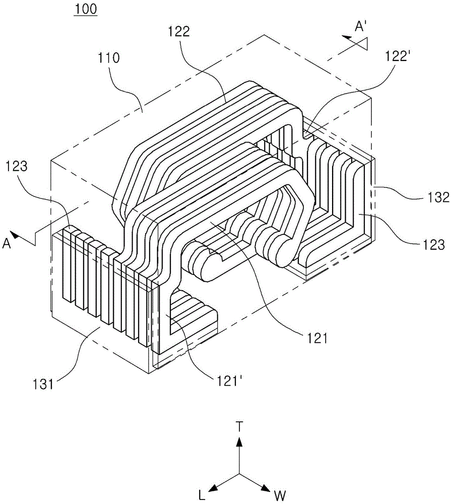
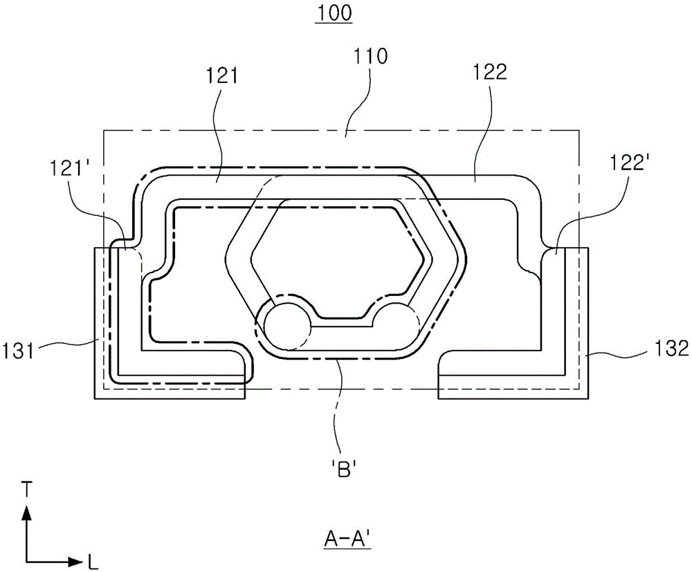
The invention discloses a stack-up electronic part and a manufacturing method thereof. The stack-up electronic part comprises a stack-up part, which is provided with a plurality of insulation layers and internal coil parts disposed on the insulation layers in a stack-up manner; an external electrode, which is disposed on the outer side of the stack-up body, and is connected with the internal coil parts. The internal coil parts are used to form step difference on a cross section in the width-thickness direction of the stack-up body.

Description

technical field [0001] The present invention relates to a laminated electronic component and its manufacturing method. Background technique [0002] Inductors, one of electronic components, are representative passive components that form circuits together with resistors and capacitors to eliminate noise, and are used in resonant circuits, filter circuits, etc., using electromagnetic characteristics and capacitors. Combining to increase the signal of a specific frequency band. [0003] In a laminated inductor, a coil pattern is formed on an insulator sheet mainly made of a magnetic material using a conductive paste or the like and laminated to form a coil inside a laminated sintered body to realize inductance. [0004] There is known a vertically laminated inductor in which an internal coil is formed in a vertical direction with respect to a substrate mounting surface in order to achieve higher inductance. Compared with a stacked inductor whose internal coils are formed alo...

Claims


Application Information

Patent Timeline
Patent Type & Authority Applications(China)
IPC IPC(8): H01F17/00H01F27/28H01F27/29H01F41/00
CPCH01F17/0006H01F17/0013H01F27/292H01F41/00H01F2017/004
Inventor 张修逢李尚锺金汉
Owner SAMSUNG ELECTRO MECHANICS CO LTD
Learn More