Nanosecond pulse width measurement device based on FPGA and method

A pulse width and measurement device technology, applied in the field of testing, can solve the problems of large printed board space, high cost, limited reference clock frequency, etc., and achieve the effect of reducing printed board space and design cost

Inactive Publication Date: 2017-03-15
THE 41ST INST OF CHINA ELECTRONICS TECH GRP
View PDF3 Cites 9 Cited by
  • Summary
  • Abstract
  • Description
  • Claims
  • Application Information

AI Technical Summary

Problems solved by technology

[0003] The existing scheme design principle adopts the method of counting the pulse width directly by the reference clock, and the minimum pulse width is limited by the frequency of the reference clock. For example, if a pulse signal of 1 nanosecond is to be measured, the counting clock required reaches 1 GHz, and there is no FPGA chip yet able to work at such high frequencies
[0004] Moreover, the existing design schemes are built with hardware circuits, which require a large number of counting chips, level conversion chips, driver chips, etc., which are costly and occupy a large space on the printed board.
[0005] At the same time, the existing design scheme is limited by the operating frequency of circuit components, and the maximum reference clock frequency is limited

Method used


Image

  • Nanosecond pulse width measurement device based on FPGA and method
  • Nanosecond pulse width measurement device based on FPGA and method
  • Nanosecond pulse width measurement device based on FPGA and method

Examples


Embodiment Construction

[0024] The following will clearly and completely describe the technical solutions in the embodiments of the present invention with reference to the accompanying drawings in the embodiments of the present invention. Obviously, the described embodiments are only some, not all, embodiments of the present invention. Based on the embodiments of the present invention, all other embodiments obtained by persons of ordinary skill in the art without making creative efforts belong to the protection scope of the present invention.

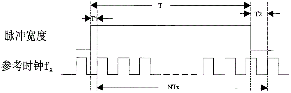
[0025] The traditional pulse width measurement uses a clock to directly count the measured pulse signal. The measurement method is limited by the clock frequency, and the minimum pulse width can only reach the order of 10 nanoseconds.

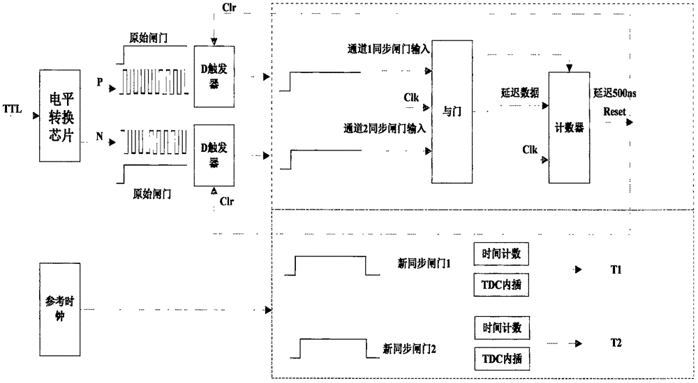
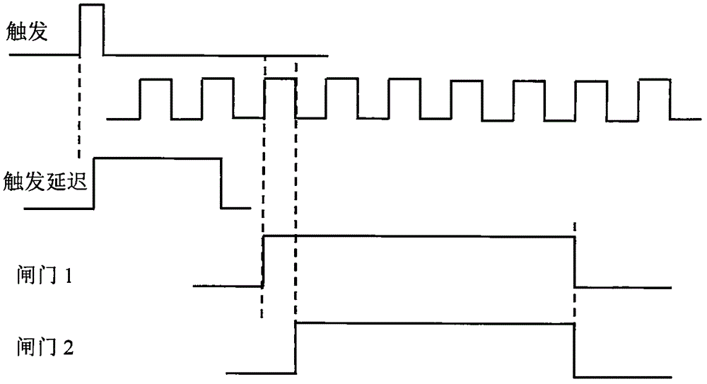
[0026] The present invention uses time counting inside the FPGA to save cost and printed board space. At the same time, it uses time intervals to measure the pulse width. in the measuring instrument.

[0027] The measuring dev...


PUM


Abstract

The invention provides a nanosecond pulse width measurement device based on a FPGA and a method. When pulse width measurement is carried out, a double-channel time interval measurement mode is employed, one channel utilizes a rising edge of an input pulse to carry out synchronization for a gate, the other channel utilizes a falling edge of the input pulse to carry out synchronization for a gate, the synchronization gates are both inputted to the FPGA, the FPGA is used for monitoring the two paths of synchronization gates, when signals of the two paths of synchronization gates are monitored to be high, after delay for a time segment, the synchronization gates of the two channels are pulled down, so the new synchronization measurement gates of the two channels are acquired, time counting and TDC interpolation compensation for the new synchronization gates inputted to the corresponding channels are carried out by each corresponding channel, and the width data of the synchronization gates is acquired; subtraction operation for the two paths of synchronization gates is carried out to acquire the pulse width data of the input pulse. The method is advantaged in that smallest pulse width which can be measured is lower than 1 nanosecond.

Description

technical field [0001] The invention relates to the technical field of testing, in particular to an FPGA-based nanosecond-level pulse width measurement device, and also relates to an FPGA-based nanosecond-level pulse width measurement method. Background technique [0002] Traditional pulse width measurement schemes such as figure 1 As shown, the clock is used to directly count the measured pulse signal, and TDC is used to perform pre-interpolation and post-interpolation compensation, and then use the formula T=NT X +T 1 -T 2 Get the pulse width value. [0003] The existing scheme design principle adopts the method of counting the pulse width directly by the reference clock, and the minimum pulse width is limited by the frequency of the reference clock. For example, if a pulse signal of 1 nanosecond is to be measured, the counting clock required reaches 1 GHz, and there is no FPGA chip yet able to work at such high frequencies. [0004] Moreover, the existing design sche...

Claims


Application Information

Patent Timeline
Patent Type & Authority Applications(China)
IPC IPC(8): G01R29/02
CPCG01R29/023
Inventor 李立功任水生杜念文刘宝东杨帆
Owner THE 41ST INST OF CHINA ELECTRONICS TECH GRP
Why Eureka
Try Eureka