A method of manufacturing a sensor with a reference capacitance
A reference capacitor and sensor technology, applied in radiation control devices, etc., can solve the problem of increasing the thickness of the sensor, and achieve the effect of eliminating the need for circuit boards, ensuring thinner, and reducing thickness
- Summary
- Abstract
- Description
- Claims
- Application Information
AI Technical Summary
Problems solved by technology
Method used
Image
Examples
Embodiment Construction
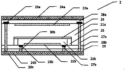
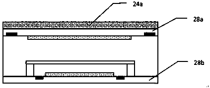
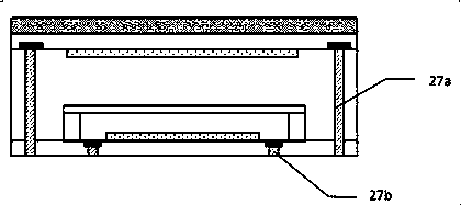
[0027] see Figure 2-8 , a sensing device 2 with a reference capacitance, comprising:
[0028] A first substrate 21a, which may be a silicon substrate, on which electronic elements (semiconductor elements) are formed, said first substrate 21a comprising a front surface having a first semiconductor element 22a and a back surface opposite to said front surface;
[0029] The groove 25 on the back side of the first substrate 21a, the depth of the groove 25 is less than or equal to half of the thickness of the first substrate, and the bottom of the groove 25 should be far away from the first semiconductor element 22a ;
[0030] The second substrate 21b fixed on the bottom of the groove 25, the second substrate 21b includes a front with the second semiconductor element 22b and a back opposite to the front, the front of the second substrate 21b is in contact with the front The back side of the first substrate 21a is coplanar;
[0031] The capacitor parallel to the side surface of ...
PUM
 Abstract
Description
Claims
Application Information
 - R&D
- Intellectual Property
- Life Sciences
- Materials
- Tech Scout
- Unparalleled Data Quality
- Higher Quality Content
- 60% Fewer Hallucinations
Browse by: Latest US Patents, China's latest patents, Technical Efficacy Thesaurus, Application Domain, Technology Topic, Popular Technical Reports.
© 2025 PatSnap. All rights reserved.Legal|Privacy policy|Modern Slavery Act Transparency Statement|Sitemap|About US| Contact US: help@patsnap.com


