A speed hierarchical optimization structure and method for improving the output of high-performance integrated circuits

A speed grading and integrated circuit technology, applied in electrical digital data processing, instruments, calculations, etc., can solve problems such as the inconsistency of the maximum operating speed of integrated circuits, and achieve the effect of increasing profits, increasing overall profits, and increasing proportions

Active Publication Date: 2019-08-06
BEIHANG UNIV
View PDF5 Cites 0 Cited by
  • Summary
  • Abstract
  • Description
  • Claims
  • Application Information

AI Technical Summary

Problems solved by technology

For example, the working clock of the originally designed integrated circuit is 20ns, and the delay of the path with the longest delay in the chip is 19ns. However, due to the influence of process errors, for different batches of integrated circuits, the delay of this path may be 21ns. It may also be 15ns, so the working clock of the integrated circuit may be above 20ns, or below 20ns, which means that the maximum operating speed of different individuals of the same integrated circuit is inconsistent

Method used


Image

  • A speed hierarchical optimization structure and method for improving the output of high-performance integrated circuits
  • A speed hierarchical optimization structure and method for improving the output of high-performance integrated circuits
  • A speed hierarchical optimization structure and method for improving the output of high-performance integrated circuits

Examples


Embodiment 1

[0100] Use the speed grading optimization structure inside the integrated circuit chip designed in the present invention to test:

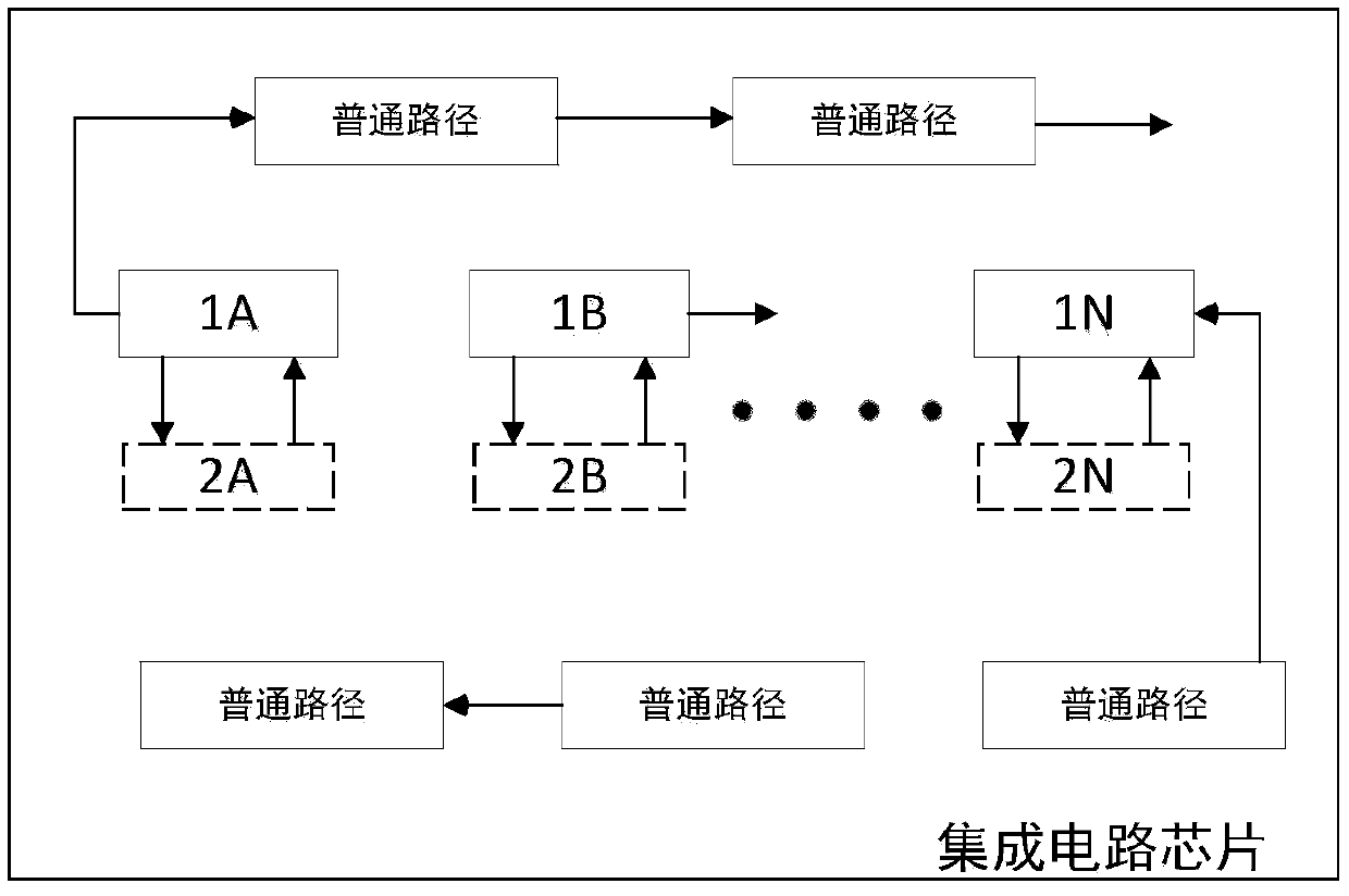
[0101] The internal speed grading optimization structure of the integrated circuit chip proposed by the present invention is inserted into several test circuits, such as the FGU (Floating Point and Graphic Unit) module in the OpenSPARCT2 processor, ITC'99 The largest circuit b19, and s953, s9234, s13207, s38417, and s35932 in the ISCAS'89 test circuit. The above-mentioned circuits inserted into the on-chip adjustment structure have been simulated and verified and verified on Altera's 28nm FPGA.

[0102] First test the single path speed grading optimization structure. A path is extracted in the b19 circuit, and the delay of this path is 851ps. The extraction method is: first use Synopsys’ Design Compiler software to synthesize the b19 test circuit, add timing constraints, convert the RTL-level code into a gate-level netlist (netlist), and generate a t...


PUM


Abstract

The invention relates to a speed grading optimization structure and method capable of improving the yield of high-performance integrated circuits. The structure is embedded in an integrated circuit and is characterized in that an integrated circuit chip comprises N critical paths, i.e., critical path A, critical path B...critical path N, which jointly form a critical path set [A, B...N], the time delay of the N paths decides the speed grading of the integrated circuit. The adopted method comprises the following steps of: 1. selecting critical paths; 2. inserting an integrated circuit speed grading optimization structure; 3. testing an integrated circuit chip at a frequency boundary Fi; 4) obtaining an original speed grading result; 5. performing speed grading optimization; 6. testing again at the frequency boundary Fi; 7. re-dividing the speed grade of the integrated circuit chip; 8. deciding the speed grade and calculating a speed grading optimization rate; 9. marking the speed grade and working frequency of the integrated chip.

Description

Technical field [0001] The invention relates to an integrated circuit chip speed grading optimization structure and optimization method, more specifically, a speed grading optimization structure suitable for improving the output of high-performance integrated circuit chips during the speed grading process of integrated circuit chips and its performance Optimized method. Background technique [0002] An integrated circuit is a kind of miniature electronic device or component. It is through the semiconductor manufacturing processes of oxidation, photolithography, diffusion, epitaxy, and aluminum evaporation, the semiconductor, resistor, capacitor and other components required to form a circuit with a certain function and the connecting wires between them are all integrated into a small piece of silicon On-chip, then solder the electronic devices packaged in a tube case; all of the components have been structured as a whole, making the electronic components a big step towards minia...

Claims


Application Information

Patent Timeline
Patent Type & Authority Patents(China)
IPC IPC(8): G06F17/50
CPCG06F30/398
Inventor 王晓晓张东嵘苏东林谢树果
Owner BEIHANG UNIV
Why Eureka
Try Eureka