Output method of pixel sensitivity value
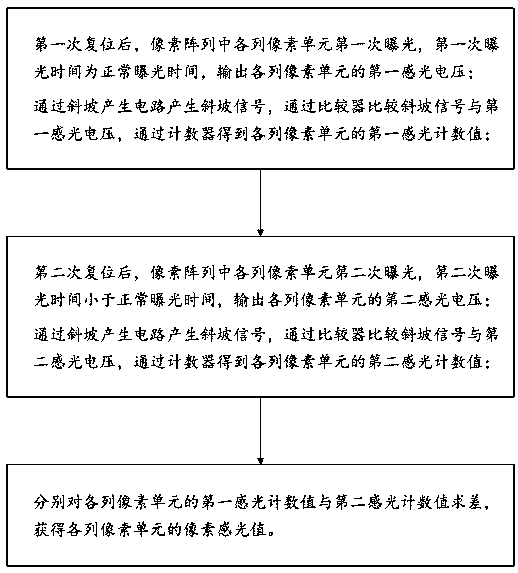
An output method and technology of photosensitive value, applied in the field of image sensor, can solve the problem that FPN cannot be effectively eliminated, and achieve the effect of eliminating fixed pattern noise and improving image quality
- Summary
- Abstract
- Description
- Claims
- Application Information
AI Technical Summary
Problems solved by technology
Method used
Image
Examples
Embodiment 1
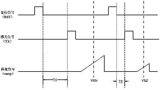
[0057] figure 2 is a timing diagram of a method for outputting a pixel sensitivity value according to Embodiment 1 of the present invention.
[0058] Such as figure 2 As shown, the RST signal is the reset control signal of the pixel photosensitive unit, the TX signal is the exposure transmission control signal of the pixel photosensitive unit, and ramp is the ramp signal generated by the ramp generating circuit.
[0059] First, the RST signal controls the pixel units of each column to reset for the first time, and then the TX signal controls the pixel units of each column to be exposed for the first time. The first exposure time T1 is the normal exposure time, and the pixel units of each column output the first photosensitive voltage respectively. The ramp generating circuit generates a first ramp signal, and the counter starts counting from zero. As the first ramp signal gradually increases, the voltage difference between the first ramp signal and the first photosensitive ...
Embodiment 2
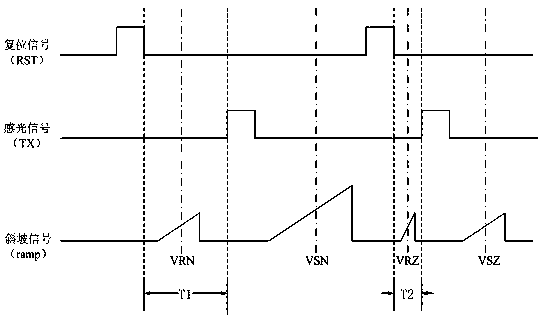
[0064] image 3 It is a timing diagram of the pixel sensitivity value output method according to the second embodiment of the present invention.
[0065] Such as image 3 As shown, the RST signal is the reset control signal of the pixel photosensitive unit, the TX signal is the exposure transmission control signal of the pixel photosensitive unit, and ramp is the ramp signal generated by the ramp generating circuit.
[0066] Firstly, the RST signal controls the pixel units in each column to reset for the first time, and the pixel units in each column output the first reset voltage respectively. The ramp generating circuit generates a first ramp signal, and the counter starts counting from zero. As the first ramp signal gradually increases, the voltage difference between the first ramp signal and the first reset voltage gradually decreases. When the When the first ramp signal exceeds the first reset voltage, the comparator is triggered to reverse, and the count value of the c...
PUM
 Abstract
Description
Claims
Application Information
 - R&D
- Intellectual Property
- Life Sciences
- Materials
- Tech Scout
- Unparalleled Data Quality
- Higher Quality Content
- 60% Fewer Hallucinations
Browse by: Latest US Patents, China's latest patents, Technical Efficacy Thesaurus, Application Domain, Technology Topic, Popular Technical Reports.
© 2025 PatSnap. All rights reserved.Legal|Privacy policy|Modern Slavery Act Transparency Statement|Sitemap|About US| Contact US: help@patsnap.com


