
A switch matrix driving circuit and method

A drive circuit and switch matrix technology, applied in electronic switches, electrical components, pulse technology, etc., can solve the problems of small expandable space of switch matrix, board-level resource occupation, difficulty in adapting to test requirements, etc., to achieve versatility and reliability Scalability, reduction of occupied resources and space, and the effect of meeting miniaturization design requirements

Active Publication Date: 2019-01-04
THE 41ST INST OF CHINA ELECTRONICS TECH GRP
View PDF4 Cites 0 Cited by
  • Summary
  • Abstract
  • Description
  • Claims
  • Application Information

AI Technical Summary

Problems solved by technology

[0003] Traditional large-scale switch matrix, due to the variety and complexity of relays and control circuits, it is difficult to realize the miniaturization of the device, occupying a lot of space resources, which is not conducive to the construction of automatic test systems
[0004] In the traditional switch matrix device, the control line is directly connected to the relay array after being boosted and expanded by the driver. In order to achieve precise control of the switch channel, all control signals of the drive circuit need to be controlled by a separate control signal line, which takes up a lot of space. Board-level resources make the expandable space of the switch matrix very small, and it is difficult to adapt to the test requirements of rapid development
[0005] The traditional switch matrix control method cannot reasonably share the control signals of the driver chip, and the sharing of control signals will cause a large number of relay misoperations, which cannot realize precise control of signal transmission and routing, and cannot guarantee the switching and routing of signal input and output in the test system
[0006] In the traditional switch matrix control method, when it is necessary to maintain the control signal state of a relay, the control signal state of the corresponding driver chip must be maintained. During long-term operation, the power loss caused is very large, and it is not conducive to the heat dissipation of the device.

Method used


Image

  • A switch matrix driving circuit and method
  • A switch matrix driving circuit and method
  • A switch matrix driving circuit and method

Examples


Embodiment Construction

[0029] The present invention will be further described below in conjunction with the accompanying drawings and embodiments.

[0030] In the prior art, each driver chip uses separate chip selection, switch level, and address data to realize the operation. However, with the expansion of the scale of the switch matrix, a huge number of control signals will be required to control the switch matrix. Therefore, In order to minimize the utilization of control circuit resources, the present invention provides a switch matrix driving circuit and method, which can realize effective utilization of control circuit resources.

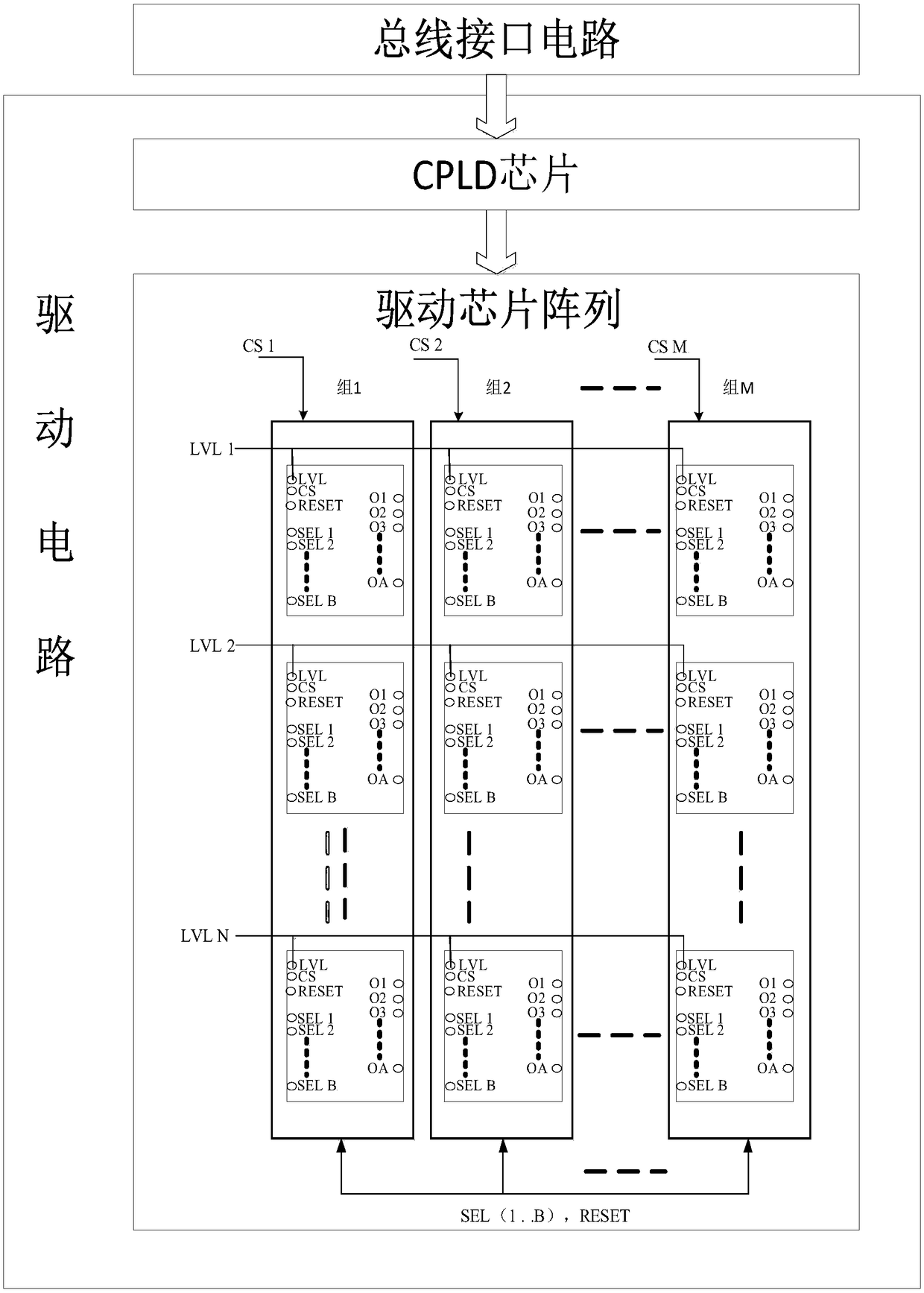
[0031] Such as figure 2 As shown, a switch matrix drive circuit, including:

[0032] The CPLD chip is used to receive the instructions sent by the bus interface and decode the received instructions;

[0033] The relay driver chip is connected with the CPLD chip through the line, and is used to receive the instruction decoded by the CPLD chip, and select the outpu...


PUM


Abstract

The invention discloses a switch matrix drive circuit and method, a CPLD chip used to receive instructions sent by a bus interface and decode the received instructions; a relay drive chip connected to the CPLD chip through a line and used to receive the CPLD The instructions decoded by the chip are selected to output valid bits through address data SEL decoding to control the corresponding relay action; wherein, the relay driver chips are M groups, any group includes N driver chips, and the driver chips of the same group share one For chip selection CS, the nth chips in different groups share a switch level signal LVL, and all drive chips share an address data SEL, where n≤N. The beneficial effects of the present invention are: by rationally designing the drive circuit and sharing the control signals in groups, the misoperation problem caused by the sharing of the control signals is effectively solved; the design integration degree of the switch matrix is ​​improved, and the miniaturization design requirement of the automatic test equipment is met.

Description

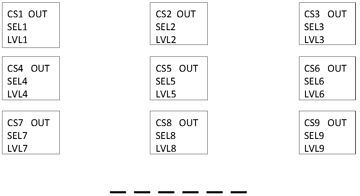
technical field [0001] The invention relates to the field of switch matrix control, in particular to a switch matrix driving circuit and method. Background technique [0002] Currently, existing switch matrix control methods such as figure 1 As shown, the driver chip has no data selection function, so the number of SEL signals can only drive the same number of relays, and it is difficult to effectively simplify the driving circuit. The control signal of the driver chip corresponds to the driver chip one by one and cannot be shared. For each additional driver chip, the corresponding chip selection and switch level control signals need to be added. The main control chip needs to allocate many more pins to control these driver chips. [0003] The traditional large-scale switch matrix, due to the variety and complexity of relays and control circuits, is difficult to realize the miniaturization of the device, takes up a lot of space resources, and is not conducive to the constru...

Claims


Application Information

Patent Timeline
Patent Type & Authority Patents(China)
IPC IPC(8): H03K17/00
CPCH03K17/002
Inventor 曹宁刘军智白月胜白亮孙建
Owner THE 41ST INST OF CHINA ELECTRONICS TECH GRP
Learn More