Pixel circuit, driving method thereof and relevant apparatus
A pixel circuit and drive transistor technology, applied in static indicators, instruments, etc., can solve problems such as uneven brightness, uneven display brightness, and current differences in different display areas
- Summary
- Abstract
- Description
- Claims
- Application Information
AI Technical Summary
Problems solved by technology
Method used
Image
Examples
Embodiment 1
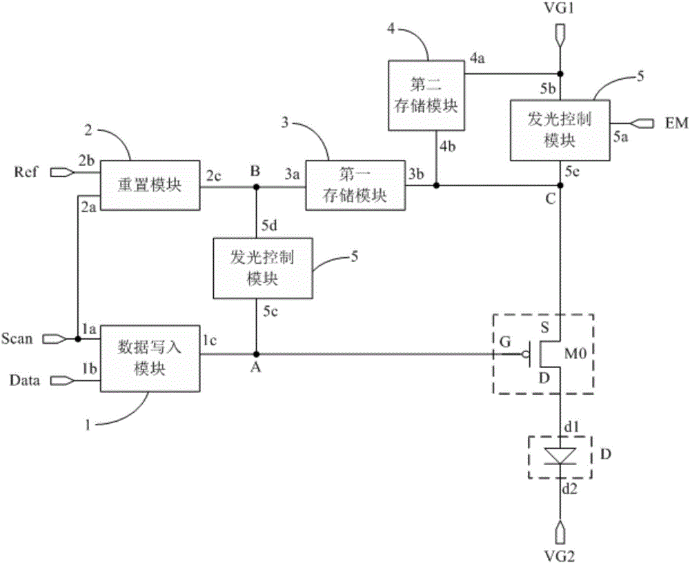
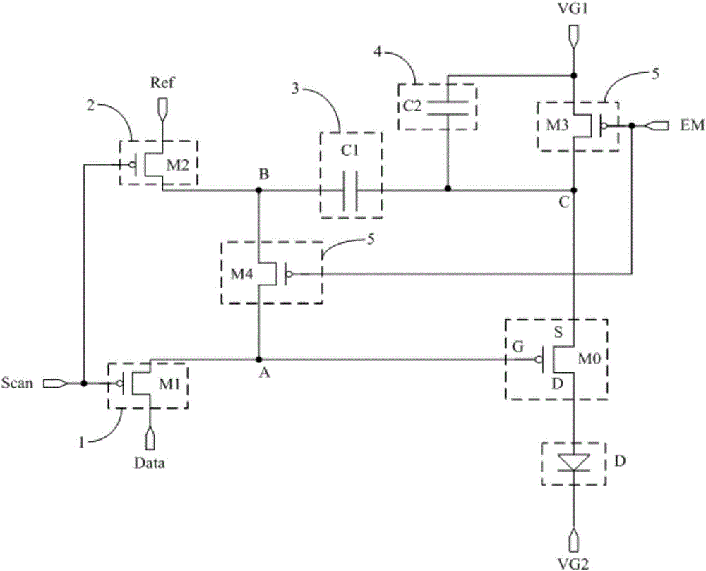
[0098] Such as Figure 2a As shown, the driving transistor M0 is a P-type transistor, and its threshold voltage V th Negative value, all switching transistors are P-type transistors; each switching transistor is cut off under the action of high potential, and turned on under the action of low potential; the first power supply terminal VG1 is positive, which means high potential, and the second power supply terminal VG2 is grounded That is, low potential; the corresponding input timing diagram is as follows Figure 4a shown. Specifically, choose the Figure 4a The three stages T1, T2 and T3 in the input timing diagram are shown.
[0099] In the T1 stage, Scan=1, EM=0. The equivalent circuit diagram is as Figure 5a shown.
[0100] Since Scan=1, both the first switch transistor M1 and the second switch transistor M2 are turned off; since EM=0, both the third switch transistor M3 and the fourth switch transistor M4 are turned on. The turned-on fourth switch transistor M4 t...
Embodiment 2
[0107] Such as Figure 3a As shown, the driving transistor M0 is an N-type transistor, and its threshold voltage V th is a positive value, all switching transistors are N-type transistors; each switching transistor is cut off under the action of a high potential, and is turned on under the action of a low potential; the first power supply terminal VG1 is grounded to be a low potential, and the second power supply terminal VG2 is a positive value That is, high potential; the corresponding input timing diagram is as follows Figure 4b shown. Specifically, choose the Figure 4b The three stages T1, T2 and T3 in the input timing diagram are shown.
[0108] In the T1 stage, Scan=0, EM=1. The equivalent circuit diagram is as Figure 6a shown.
[0109] Since Scan=0, both the first switch transistor M1 and the second switch transistor M2 are turned off; since EM=1, both the third switch transistor M3 and the fourth switch transistor M4 are turned on. The turned-on fourth switch...
PUM
 Abstract
Description
Claims
Application Information
 - R&D
- Intellectual Property
- Life Sciences
- Materials
- Tech Scout
- Unparalleled Data Quality
- Higher Quality Content
- 60% Fewer Hallucinations
Browse by: Latest US Patents, China's latest patents, Technical Efficacy Thesaurus, Application Domain, Technology Topic, Popular Technical Reports.
© 2025 PatSnap. All rights reserved.Legal|Privacy policy|Modern Slavery Act Transparency Statement|Sitemap|About US| Contact US: help@patsnap.com


