Grooved gate VDMOS

A trench gate and well region technology is applied to trench gate VDMOS. It can solve problems such as SEB and SEGR, and achieve the effect of avoiding charge diffusion, improving reliability and reducing risks.

Active Publication Date: 2016-11-09
北京中科微投资管理有限责任公司
View PDF4 Cites 4 Cited by
  • Summary
  • Abstract
  • Description
  • Claims
  • Application Information

AI Technical Summary

Problems solved by technology

[0005] By providing a trench gate VDMOS, the present invention solves the technical problem that SEB and SEGR are prone to occur in the trench gate VDMOS using the charge coupling technology in the prior art

Method used


Image

  • Grooved gate VDMOS
  • Grooved gate VDMOS
  • Grooved gate VDMOS

Examples


Embodiment Construction

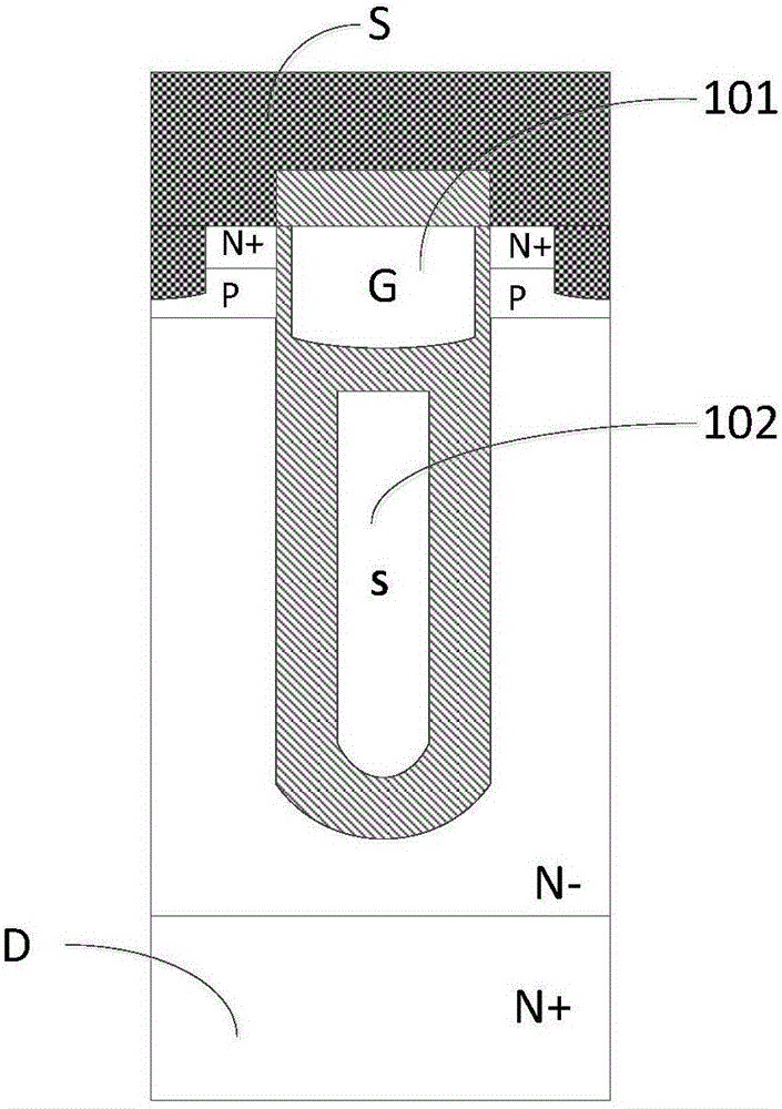
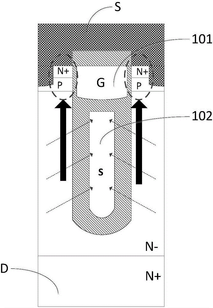
[0024] The embodiment of the present application provides a trench gate VDMOS, which solves the technical problem that SEB and SEGR are prone to occur in the trench gate VDMOS using charge coupling technology in the prior art. The technical effect of reducing the risk of SEB and SEGR and improving reliability is realized.

[0025] In order to solve the above technical problems, the general idea of ​​the technical solution provided by the embodiment of the present application is as follows:

[0026] The present application provides a trench gate VDMOS, including:

[0027] A substrate, an epitaxial layer, a first well region located on the surface of the epitaxial layer, a second well region located on the surface of the first well region, a first source electrode located on the surface of the second well region, and a grooved gate , a gate oxide layer surrounding the trench gate, a second source vertical field plate, and a silicon dioxide layer surrounding the second source ve...


PUM


Abstract

The invention discloses a grooved gate VDMOS, which comprises a substrate, an epitaxial layer, a first well region, a second well region, a first source located on the surface of the second well region, a grooved gate, a gate oxide layer surrounding the grooved gate, a second source longitudinal field plate and a silicon dioxide layer surrounding the second source longitudinal field plate, wherein the substrate, the epitaxial layer and the second well region all have first doping types; the first well region has a second doping type; and the gate oxide layer and the silicon dioxide layer are isolated by the first well region and the second well region. The grooved gate VDMOS provided by the invention aims at solving the technical problems that in the case of space radiation existing in the grooved gate VDMOS by applying a charge coupling technology in the prior art, SEB (Singer Even Burnout) and SEGR (Single Event Gate Rupture) are likely to happen. Technical effects of reducing SEB and SEGR risks and improving the reliability are realized.

Description

technical field [0001] The invention relates to the field of semiconductors, in particular to a trench gate VDMOS. Background technique [0002] In the field of semiconductors, the MOSFET device whose gate is made by trenching technology is called trench gate VDMOS. Because trench gate VDMOS has higher power density and lower on-resistance than traditional VDMOS in the field of medium and low voltage applications, it has been obtained a wide range of applications. And in the field of medium voltage, such as figure 1 As shown, generally on the basis of the trench gate 101, the charge coupling technology is introduced, that is, the lateral electric field formed by the coupling effect of the vertical field plate called the second source 102 deep into the silicon epitaxial layer and the carrier in the silicon , reduce the dependence between breakdown voltage and on-resistance, and improve device performance. [0003] However, when it is applied in the aerospace field, due to ...

Claims


Application Information

Patent Timeline
Patent Type & Authority Applications(China)
IPC IPC(8): H01L29/78H01L29/08
CPCH01L29/086H01L29/7813
Inventor 孙博韬王立新丁艳
Owner 北京中科微投资管理有限责任公司
Why Eureka
Try Eureka