MPC8640D based information processing board system
A technology of MPC8640D and PEX8648, applied in the field of information processing board system based on MPC8640D, can solve the problems of poor reliability and high power consumption, and achieve the effect of enhanced reading ability, low power consumption and high data interaction speed
- Summary
- Abstract
- Description
- Claims
- Application Information
AI Technical Summary
Problems solved by technology
Method used
Image
Examples
Embodiment 1
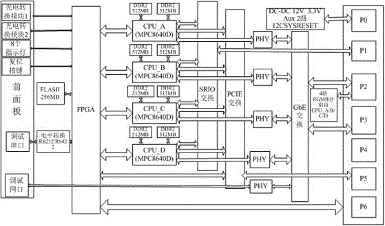
[0021] Such as figure 1 As shown, an information processing board system based on MPC8640D includes an FPGA, and the FPGA is plugged with 4 CPUs. The CPU model is MPC8640D, and each CPU is connected to the VPX connector through the SRIO bus, the PCIE bus and the GbE bus. , used for data interaction inside and outside the board, the FPGA is connected with 256MB of FLASH, and the FPGA is also connected to the two photoelectric conversion modules, the debugging serial port and the reset button on the front panel respectively.
[0022] In the present invention, one FPGA is externally connected with four MPC8640Ds for information processing. The MC8640 supports 1GHz processing capacity, adopts +0.95V core voltage, and has lower power consumption and higher reliability under the same ambient temperature and main frequency. The 256MB FLASH connected to the FPGA further enhances the ability to read information. The signal lines of the Flash are all connected to the FPGA, and the 4 Loc...
Embodiment 2
[0024] This embodiment is a further improvement made on the basis of the above embodiments, such as figure 1 As shown, in this embodiment, each CPU is connected with two DDRs, and the capacity of each DDR is 512MB. Using 8 pieces of 128MB DDR2 of model MT47H64M16-37E, each group of 4 pieces constitutes 64bit, and each processing core is plugged into a group to form dual-channel DDR2. The maximum clock frequency of MT47H64M16-37E is 333MHz. FLASH includes two pieces of S29GL01GP FLASH chips from Spansion Company. The two pieces of S29GL01GP FLASH chips are spliced into 32bit width and capacity ≥ 256MB, which improves the access speed; all the signal lines of Flash are connected to FPGA, and 4 LocalBus of MPC8640D access Flash through FPGA .
[0025] The SRIO bus includes the TS1578 chip. The TS1578 chip includes 8 x 4 SRIO interfaces, of which 4 x 4 SRIO interfaces are connected to 4 CPUs respectively, and the remaining 4 x 4 SRIO interfaces are connected to the P1 port of t...
Embodiment 3
[0029] This embodiment is a further improvement made on the basis of the above-mentioned embodiments, such as figure 1 As shown, in this embodiment, there are also 8 LED indicators on the front panel, the debugging network port is a 1000Base-T Ethernet interface, the debugging serial port is a RS232 asynchronous serial port, and each of the two photoelectric conversion modules includes 1 fiber optic interface, the default line speed of the fiber optic interface is 3.12Gbps.
PUM
 Abstract
Description
Claims
Application Information
 - R&D
- Intellectual Property
- Life Sciences
- Materials
- Tech Scout
- Unparalleled Data Quality
- Higher Quality Content
- 60% Fewer Hallucinations
Browse by: Latest US Patents, China's latest patents, Technical Efficacy Thesaurus, Application Domain, Technology Topic, Popular Technical Reports.
© 2025 PatSnap. All rights reserved.Legal|Privacy policy|Modern Slavery Act Transparency Statement|Sitemap|About US| Contact US: help@patsnap.com

