Polarization Stable Broadband Absorbing Material
An absorbing material and broadband technology, applied in the field of antenna communication, absorption shielding, and absorbing materials, can solve the problems of poor polarization stability and insufficient low-frequency bandwidth, achieve absorption and shielding, widen the working bandwidth, and increase the current. effect of path
- Summary
- Abstract
- Description
- Claims
- Application Information
AI Technical Summary
Problems solved by technology
Method used
Image
Examples
Embodiment 1
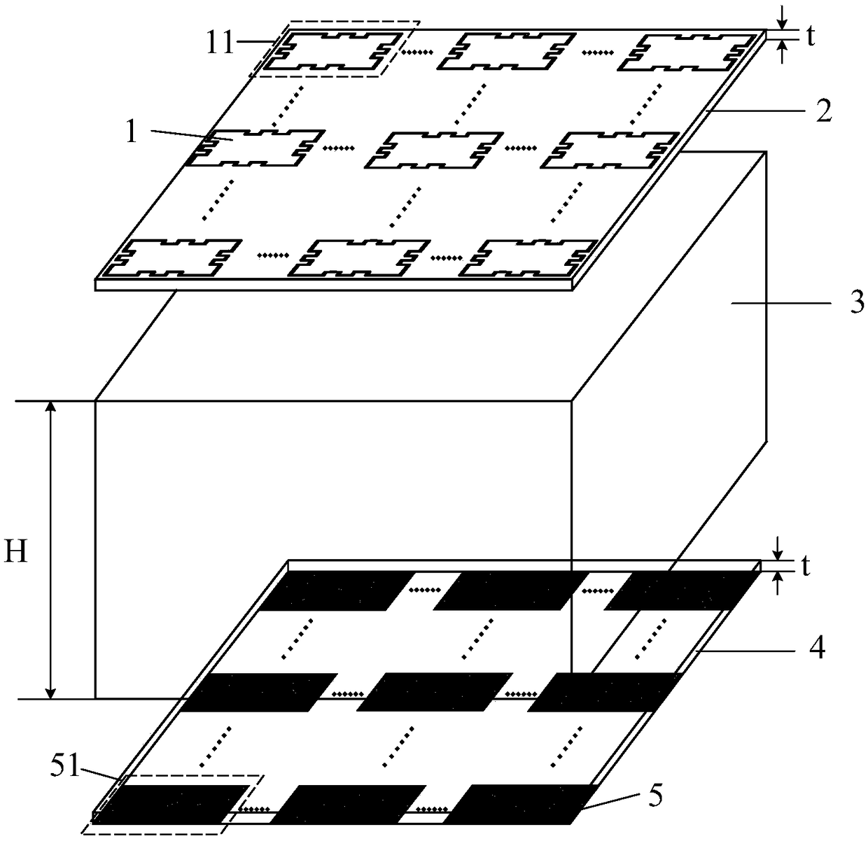
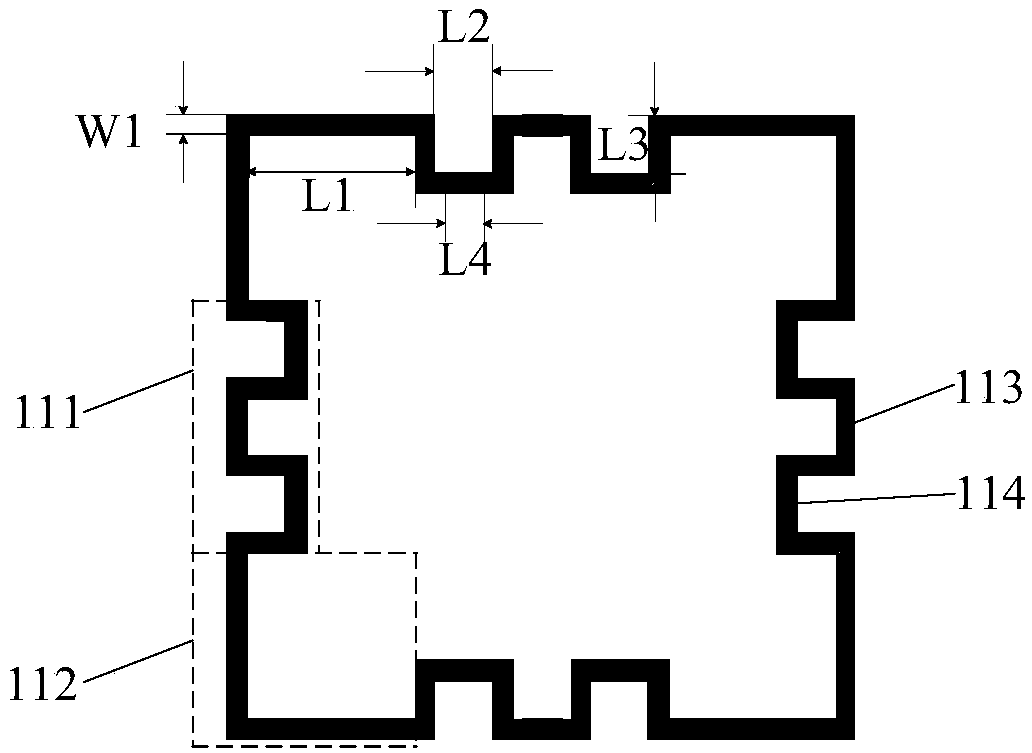
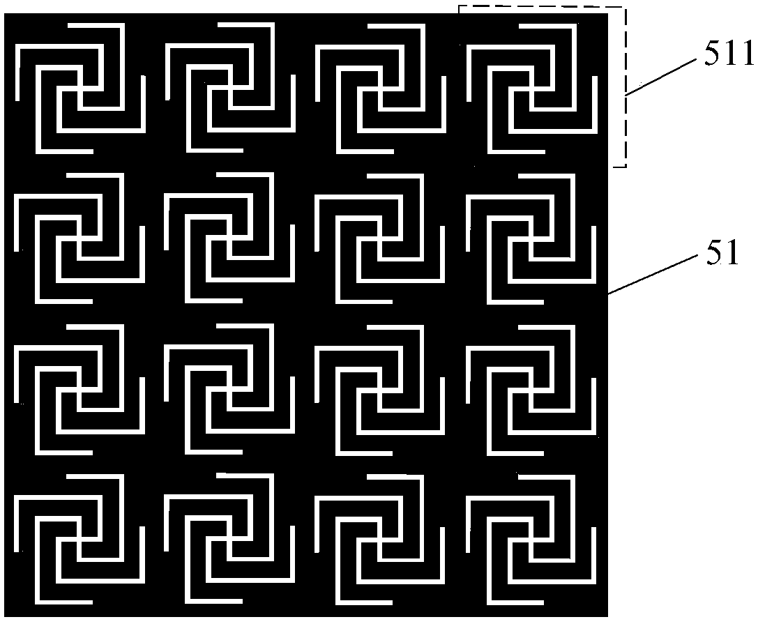
[0026] refer to figure 1 , the present invention includes a wave-absorbing structure 1, an upper dielectric plate 2, a foam layer 3, a lower dielectric plate 4 and a frequency selective surface 5; the wave-absorbing structure 1 is printed on the upper surface of the upper dielectric plate 2, and it The geometric center of the upper surface coincides; the frequency selective surface 5 is printed on the lower surface of the lower dielectric plate 4, and it coincides with the geometric center of the lower surface of the lower dielectric plate 4; the upper dielectric plate 2, the foam layer 3 and the lower dielectric plate 4 Arranged in order to form an up and down stacked structure, and the edges of the upper dielectric plate 2, the foam layer 3 and the lower dielectric plate 4 coincide with each other; the absorbing structure 1 is formed by periodic arrangement of M×N quasi-square metal folding line units 11, The frequency selective surface 5 is formed by periodic arrangement of...
Embodiment 2
[0030] The structure of embodiment 2 is identical with the structure of embodiment 1, and following parameter has been adjusted:
[0031] The arrangement periods of the metal fold line unit 11 and the frequency selective surface unit 51 are both 17 mm; the upper dielectric plate 2, the foam layer 3 and the lower dielectric plate 4 are all square plates with a side length of 170 mm, wherein the upper dielectric plate 2 and the lower dielectric plate The thickness of 4 is t=0.2mm, and the relative dielectric constant is 2.25; the metal line width W1=0.5mm of the metal folding line unit 11; the length of both arms of the equal-arm "L" type metal folding line 112 is L1=4.3mm; The width of the two grooves of the "bow"-shaped metal fold line 111 with a gap is L2=1.5mm, and the length of the gap is L4=1mm; the resistance value of the eight second chip resistors 114 is 40 ohms; the word "一" The edge distance S1 between the shaped groove 5112 and the folded line groove unit 511 is 0.22...
Embodiment 3
[0032] The structure of embodiment 3 is identical with the structure of embodiment 1, and following parameter has been adjusted:
[0033] The arrangement periods of the metal fold line unit 11 and the frequency selective surface unit 51 are both 16.2 mm; the upper dielectric plate 2, the foam layer 3 and the lower dielectric plate 4 are all square plates with a side length of 162 mm, wherein the upper dielectric plate 2 and the lower dielectric plate The thickness of plate 4 is t=0.2mm, and relative dielectric constant is 2.65; Foam layer 3 thickness H=15mm; The metal wire width W1=0.5mm of metal folding line unit 11; The length of the arm is L1=4mm; the width of the two grooves of the "bow"-shaped metal fold line 111 with the gap is L2=1.5mm, and the length of the gap is L4=1mm; the resistance value of the eight second chip resistors 114 is 40 ohms; the distance S1 between the "one"-shaped slot 5112 and the edge of the folded line slot unit 511 is 0.125mm.
[0034] Below in ...
PUM
 Abstract
Description
Claims
Application Information
 - R&D
- Intellectual Property
- Life Sciences
- Materials
- Tech Scout
- Unparalleled Data Quality
- Higher Quality Content
- 60% Fewer Hallucinations
Browse by: Latest US Patents, China's latest patents, Technical Efficacy Thesaurus, Application Domain, Technology Topic, Popular Technical Reports.
© 2025 PatSnap. All rights reserved.Legal|Privacy policy|Modern Slavery Act Transparency Statement|Sitemap|About US| Contact US: help@patsnap.com


