Integrated circuit device, manufacturing method, circuit board, display panel and display device

A technology for integrated circuits and display panels, which is applied in the fields of integrated circuit devices and their manufacturing methods, display devices, display panels, and circuit boards, and can solve the problems of unfavorable transparent display, large space, and large space occupied by silicon-based integrated circuit devices. , to achieve transparent display and optimize the effect of occupying space

Pending Publication Date: 2016-10-12
BOE TECH GRP CO LTD
View PDF6 Cites 6 Cited by
  • Summary
  • Abstract
  • Description
  • Claims
  • Application Information

AI Technical Summary

Problems solved by technology

[0005] To sum up, the silicon-based integrated circuit device in the prior art occupies a relatively large space, and most of the packaging materials in the prior art packaging are made of non-transparent materials. When the silicon-based integrated circuit device is placed on the display, it will not only occupy Larger space, and not conducive to the realization of intelligent transparent display

Method used


Image

  • Integrated circuit device, manufacturing method, circuit board, display panel and display device
  • Integrated circuit device, manufacturing method, circuit board, display panel and display device
  • Integrated circuit device, manufacturing method, circuit board, display panel and display device

Examples


Embodiment Construction

[0048] Embodiments of the present invention provide an integrated circuit device and a manufacturing method thereof, a circuit board, a display panel, and a display device, which are used to reduce the occupied space of the integrated circuit device, and when the integrated circuit device is placed on the display, it is beneficial to realize intelligent transparent display.

[0049] In order to make the purpose, technical solutions and advantages of the present invention clearer, the present invention will be further described in detail below in conjunction with the accompanying drawings. Obviously, the described embodiments are only some of the embodiments of the present invention, rather than all of them. Based on the embodiments of the present invention, all other embodiments obtained by persons of ordinary skill in the art without making creative efforts belong to the protection scope of the present invention.

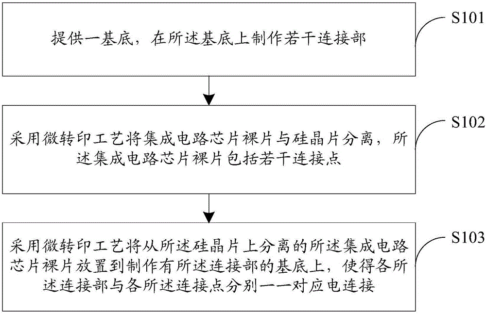
[0050] The integrated circuit device provided by the specific...


PUM

PropertyMeasurementUnit
sizeaaaaaaaaaa
sizeaaaaaaaaaa
sizeaaaaaaaaaa

Abstract

The invention discloses an integrated circuit device, a manufacturing method thereof, a circuit board, a display panel and a display device which are used for reducing space occupied by the integrated circuit device. When the integrated circuit device is arranged on a displayer, intelligent transparent display is easily achieved. The integrated circuit device comprises a substrate, a plurality of connection parts and an integrated circuit bare chip, the connection parts and the integrated circuit bare chip are arranged on the substrate, the integrated circuit bare chip comprises a plurality of connection points, and the connection parts are electrically connected with the connection points respectively in a one-to-one correspondence mode.

Description

technical field [0001] The invention relates to the field of display technology, in particular to an integrated circuit device and a manufacturing method thereof, a circuit board, a display panel, and a display device. Background technique [0002] With the rapid development of display technology, more and more functions can be realized by the display. At present, various functions are realized mainly by setting silicon-based integrated circuit devices with different functions on the display, such as: setting on the display can realize automatic Silicon-based sensors for detection and automatic control functions. [0003] The manufacturing industry chain of silicon-based integrated circuit devices mainly includes fabs and packaging and testing factories. The following will introduce silicon-based sensors as an example. Silicon-based sensors refer to integrated circuit devices with sensing functions based on silicon-based processes. The wafer factory produces sensor chip bar...

Claims


Application Information

Patent Timeline
Patent Type & Authority Applications(China)
IPC IPC(8): G02F1/133H01L27/32G09F9/00H05K1/11H05K3/32
CPCG02F1/133G09F9/00H05K1/11H05K3/32H10K59/00G02F1/13454H01L24/11H01L24/13G01R1/0433H01L21/28H01L21/31H01L23/32H05K1/147
Inventor 郭玉珍董学王海生吴俊纬刘英明丁小梁许睿李昌峰赵利军韩艳玲王鹏鹏曹学友张平刘伟贾亚楠
Owner BOE TECH GRP CO LTD
Why Eureka
Try Eureka