Anti-electromagnetic protective membrane and preparation method thereof
A protective film and anti-electromagnetic technology, applied in the direction of film/flaky adhesives, adhesive additives, non-polymer adhesive additives, etc., can solve the problems of poor compatibility between antimagnetic substances and resins, easy peeling of coatings, Complicated structure and other problems, to achieve good anti-electromagnetic effect, easy to fall off, and good compatibility
- Summary
- Abstract
- Description
- Claims
- Application Information
AI Technical Summary
Problems solved by technology
Method used
Image
Examples
Embodiment 1
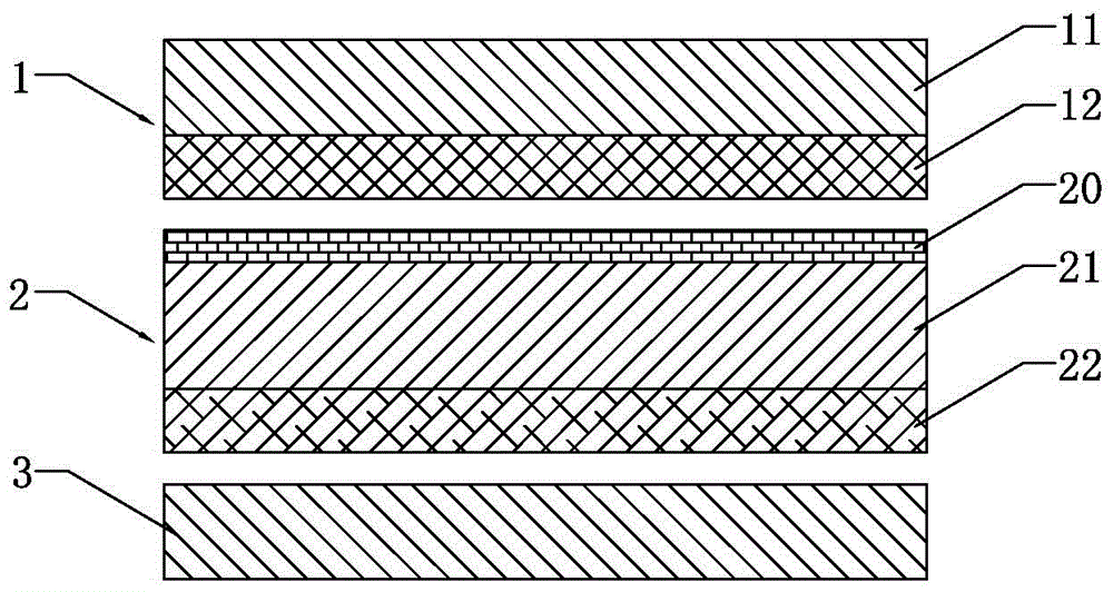
[0041] See figure 1 , an anti-electromagnetic protective film, comprising a protective film layer 1, a use film layer 2 and a release film 3 sequentially attached from top to bottom, and the protective film layer includes a protective film 11 and a release glue attached to the lower surface of the protective film 11 Layer 12, the use of film layer 2 includes a substrate 21 attached to the lower surface of the peeling adhesive layer 12 and an antimagnetic adhesive layer 22 attached to the lower surface of the substrate 21, the lower surface of the antimagnetic adhesive layer 22 and the release film The upper surface of 3 fits.
[0042] The protective film 11 and the peeling film 3 are PET films; the peeling adhesive layer 12 is a silica gel layer; the base material 21 is a PET film; Layer 20, the upper surface and the lower surface of the hardened layer 20 are attached to the lower surface of the peeling adhesive layer 12 and the upper surface of the base material 21 respectiv...
Embodiment 2
[0061] The difference between this embodiment and the above-mentioned embodiment 1 is that: the protective film 11 and the peeling film 3 are both PVC films; the peeling adhesive layer 12 is an acrylic adhesive layer; and the substrate 21 is a PVC film.
[0062] The thickness of the protective film 11 and the peeling film 3 are both 35 μm; the thickness of the peeling adhesive layer 12 is 8 μm; the thickness of the substrate 21 is 45 μm; the thickness of the antimagnetic adhesive layer 22 is 28 μm; The thickness of the hardened layer 20 is 4 μm.
[0063] The anti-magnetic bonding layer 22 is made by curing the anti-electromagnetic glue after coating, and the anti-electromagnetic glue is composed of the following raw materials in parts by weight:
[0064] Glue 100 parts
[0065] Anti-electromagnetic substance 10 parts
[0066] 0.8 parts of coupling agent
[0067] Curing agent 0.1 part
[0068] Catalyst 0.02 parts
[0069] 30 parts of solvent.
[0070] The glue is polyuret...
Embodiment 3
[0076] The difference between this embodiment and the above-mentioned embodiment 1 is that: the protective film 11 and the peeling film 3 are both PC films; the peeling adhesive layer 12 is a pressure-sensitive adhesive layer; and the substrate 21 is a PC film.
[0077] The thickness of the protective film 11 and the peeling film 3 are both 50 μm; the thickness of the peeling adhesive layer 12 is 12 μm; the thickness of the substrate 21 is 60 μm; the thickness of the antimagnetic adhesive layer 22 is 30 μm; The thickness of the hardened layer 20 is 5 μm.
[0078] The anti-magnetic bonding layer 22 is made by curing the anti-electromagnetic glue after coating, and the anti-electromagnetic glue is composed of the following raw materials in parts by weight:
[0079] Glue 100 parts
[0080] Anti-electromagnetic substance 20 parts
[0081] Coupling agent 1.0 parts
[0082] Curing agent 0.25 parts
[0083] Catalyst 0.03 parts
[0084] 35 parts of solvent.
[0085] The glue is ...
PUM
| Property | Measurement | Unit |
|---|---|---|
| Thickness | aaaaa | aaaaa |
| Thickness | aaaaa | aaaaa |
| Thickness | aaaaa | aaaaa |
Abstract
Description
Claims
Application Information
 - R&D Engineer
- R&D Manager
- IP Professional
- Industry Leading Data Capabilities
- Powerful AI technology
- Patent DNA Extraction
Browse by: Latest US Patents, China's latest patents, Technical Efficacy Thesaurus, Application Domain, Technology Topic, Popular Technical Reports.
© 2024 PatSnap. All rights reserved.Legal|Privacy policy|Modern Slavery Act Transparency Statement|Sitemap|About US| Contact US: help@patsnap.com


