A dc-dc conversion circuit
A technology of DC-DC and conversion circuits, which is applied in the direction of converting DC power input to DC power output, electrical components, and adjusting electrical variables. It can solve the problems of large common-mode interference, high implementation cost, and high voltage requirements, and achieve reduction Current ripple, reduce the difficulty of implementation, reduce the effect of the filter
- Summary
- Abstract
- Description
- Claims
- Application Information
AI Technical Summary
Problems solved by technology
Method used
Image
Examples
Embodiment 1
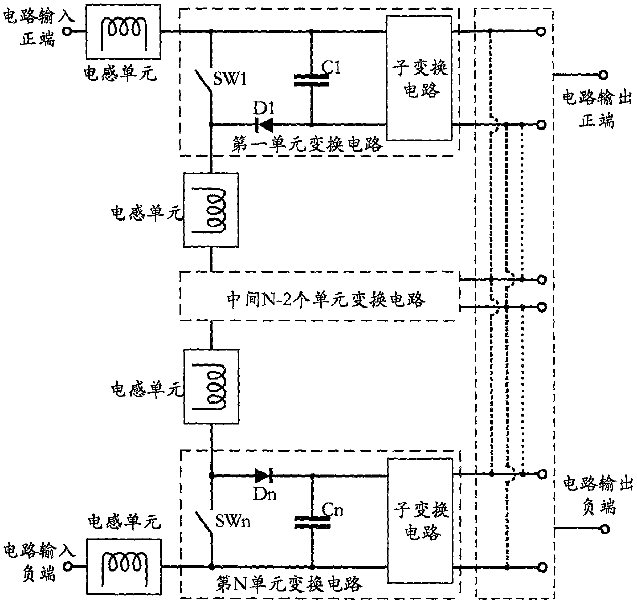
[0019] Such as figure 1 As shown, it is a DC-DC conversion circuit, including: N unit conversion circuits, M inductance units, circuit input positive terminals, circuit input negative terminals, circuit output positive terminals and circuit output negative terminals, the first unit The positive input terminal of the conversion circuit is connected to the positive input terminal of the circuit through an inductance unit or directly, and the negative input terminal of the conversion circuit of the Kth unit is connected to the positive input terminal of the K+1th unit conversion circuit through an inductance unit or directly. connection, K, M and N are natural numbers, K
Embodiment 2
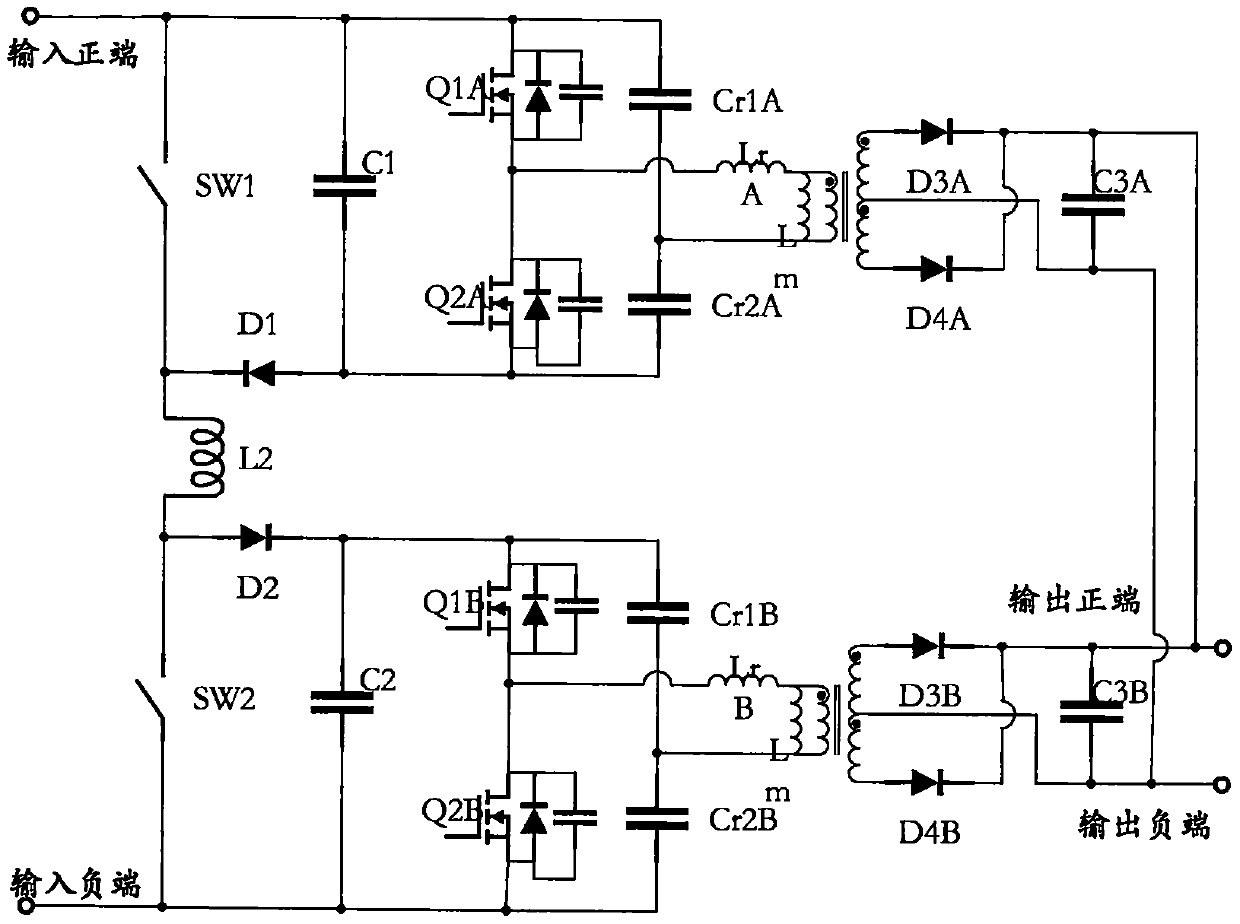
[0038] Such as figure 2 As shown, it is a schematic diagram of the second embodiment of the present invention, the number of unit conversion circuits N is 2, an inductance unit is selected for the inductance unit and connected in series between the first unit circuit and the second unit circuit, and the positive input terminal is directly connected to the first unit circuit. One end of the unit circuit is connected, and the input negative terminal is directly connected to one end of the second unit circuit, so that there is no high-frequency voltage jitter between C1 and C2 and the input, and the best effect of eliminating common mode interference is achieved; in the first and second unit circuits The commonly used half-bridge LLC circuit is selected for the sub-conversion circuit, and its output terminal is connected in parallel; by the half-bridge LLC voltage gain formula
[0039]
[0040] It can be seen that, apart from the parameter design (resonant cavity parameters L...
Embodiment 3
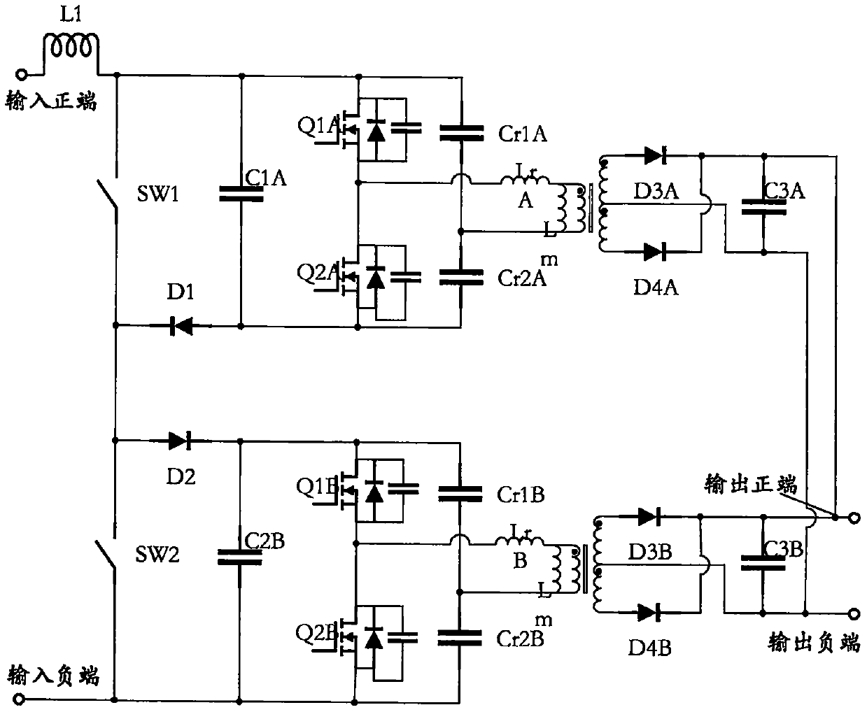
[0045] Such as image 3 As shown, it is a schematic diagram of the third embodiment of the present invention. The circuit takes the number of circuit groups N as 2, and the inductance unit selects an inductance unit and connects it in series between the positive input terminal and the first unit circuit. The first and second unit The circuits are directly connected in series, and the input negative terminal is directly connected with one terminal of the second unit circuit. The sub-converting circuits in the first and second unit circuits also select the commonly used half-bridge LLC circuit, and the output ends are connected in parallel. In this way, the voltage of C2 has no high-frequency jitter relative to the input, but the voltage of C1 has high-frequency jitter relative to the input. Therefore, for the problem of common-mode interference, this embodiment only reduces the common-mode interference, which is a suboptimal solution compared to the first embodiment. Like the ...
PUM
 Abstract
Description
Claims
Application Information
 - R&D
- Intellectual Property
- Life Sciences
- Materials
- Tech Scout
- Unparalleled Data Quality
- Higher Quality Content
- 60% Fewer Hallucinations
Browse by: Latest US Patents, China's latest patents, Technical Efficacy Thesaurus, Application Domain, Technology Topic, Popular Technical Reports.
© 2025 PatSnap. All rights reserved.Legal|Privacy policy|Modern Slavery Act Transparency Statement|Sitemap|About US| Contact US: help@patsnap.com


