
Three-stage transconductance amplifier

A technology of transconductance amplifier and input structure, applied in amplifiers, differential amplifiers, amplifiers with semiconductor devices/discharge tubes, etc., can solve the problems of increased layout area, low voltage slew rate of transconductance amplifiers, and reduced dominant pole frequency , to achieve the effect of increasing the unity gain bandwidth, maximizing, and increasing the voltage slew rate

Active Publication Date: 2016-08-24
NO 24 RES INST OF CETC
View PDF3 Cites 2 Cited by
  • Summary
  • Abstract
  • Description
  • Claims
  • Application Information

AI Technical Summary

Problems solved by technology

However, the frequency of the first non-dominant pole is usually low, and the frequency of the left-half-plane zero generated by the traditional method is relatively high, which requires a large compensation capacitor design, which will lead to an increase in the layout area on the one hand. On the other hand, it will also reduce the dominant pole frequency, thereby reducing the -3dB bandwidth and unity gain bandwidth, so that the voltage slew rate of the transconductance amplifier is still low, which cannot change the current situation that the quality factor of the transconductance amplifier is still not high

Method used


Image

  • Three-stage transconductance amplifier
  • Three-stage transconductance amplifier
  • Three-stage transconductance amplifier

Examples


Embodiment Construction

[0026] The preferred embodiments of the present invention will be described in detail below in conjunction with the accompanying drawings; it should be understood that the preferred embodiments are only for illustrating the present invention, rather than limiting the protection scope of the present invention.

[0027] In order to describe the above problems in more detail, first analyze the working principle of the two three-stage transconductance amplifiers and the advantages and disadvantages of frequency compensation technology.

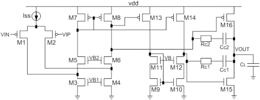
[0028] Such as figure 1 A schematic diagram of a traditional three-stage transconductance amplifier RC compensation technology (referred to as the structure [1]) is given. The two compensation networks are respectively composed of compensation resistor Rc1 / compensation capacitor Cc1 and compensation resistor Rc2 / compensation capacitor Cc2 in series. One end of the compensation resistor Rc1 is connected to the compensation capacitor Cc1, the other ...


PUM


Abstract

The invention relates to a three-stage transconductance amplifier design. The three-stage transconductance amplifier is characterized in that NMOS (N-channel Metal Oxide Semiconductor) tubes M3 / M4 / M5 / M6, PMOS (P-channel Metal Oxide Semiconductor) tubes M1 / M2 / M7 / M8 and a tail current source Iss form a folding input structure and a first stage; NMOS tubes M9 / M10 / M11 / M12 and PMOS tubes M13 / M14 form a second stage; an NMOS tube M15 and a PMOS tube M16 form a third stage; NMOS tubes M17 / M18, PMOS tubes M19 / M20 and a capacitor Cc form a compensation structure; the input end of the compensation structure is connected to the output end of the second stage of the transconductance amplifier; and the output end of the compensation structure is connected to the output end of the transconductance amplifier. A power supply of the transconductance amplifier is vdd1, a power supply of the compensation structure is vdd2 and a capacitor CL represents a load capacitor of the transconductance amplifier. According to the three-stage transconductance amplifier, a left half plane zero is introduced into a product of a gain A of a gain stage and the capacitor Cc, so that a dominant pole of a transmission function of the three-stage transconductance amplifier is not reduced, and the transconductance amplifier is guaranteed to have relatively large -3dB bandwidth and unity-gain bandwidth.

Description

technical field [0001] The invention belongs to the technical field of analog or digital-analog hybrid integrated circuits, and relates to the design and frequency compensation technology of a three-stage transconductance amplifier. Background technique [0002] In recent years, with the continuous development of integrated circuit design technology, more and more transconductance amplifiers are used in the field of analog integrated circuit design. With the continuous improvement of integrated circuit manufacturing technology, the power supply voltage continues to decrease. The sleeve-type gain stage structure formed in series will significantly compress the voltage swing of the transconductance amplifier, which is not suitable for the application under the power supply voltage. The cascade structure of multiple gain stages can effectively achieve the purpose of high gain. At the same time, Under low power supply voltage, it can effectively maintain a large voltage swing. ...

Claims


Application Information

Patent Timeline
Patent Type & Authority Applications(China)
IPC IPC(8): H03F3/45
CPCH03F3/45107
Inventor 徐代果胡刚毅李儒章王健安刘涛刘璐邓民明石寒夫王旭
Owner NO 24 RES INST OF CETC
Learn More