
Inductively coupled transformer with tunable impedance match network

A technology of inductors and networks, applied in the field of input matching of RF power transistors, can solve problems such as inability to compensate, additional cost and complexity

Active Publication Date: 2016-08-17
沃孚半导体公司
View PDF5 Cites 3 Cited by
  • Summary
  • Abstract
  • Description
  • Claims
  • Application Information

AI Technical Summary

Problems solved by technology

However, these techniques introduce additional cost and complexity, and cannot compensate for all possible effects from the rated

Method used


Image

  • Inductively coupled transformer with tunable impedance match network
  • Inductively coupled transformer with tunable impedance match network
  • Inductively coupled transformer with tunable impedance match network

Examples


Embodiment Construction

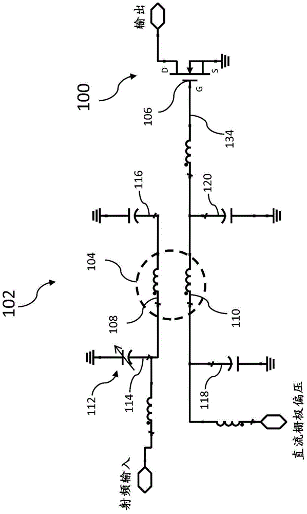
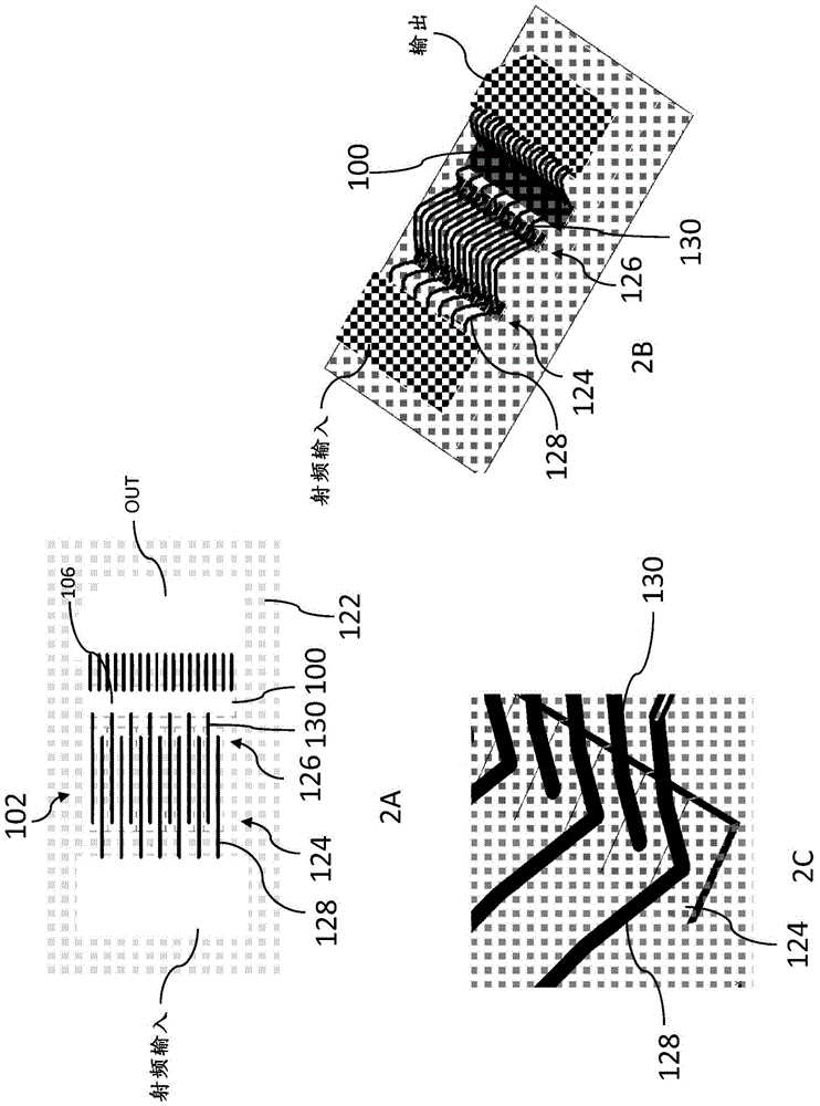
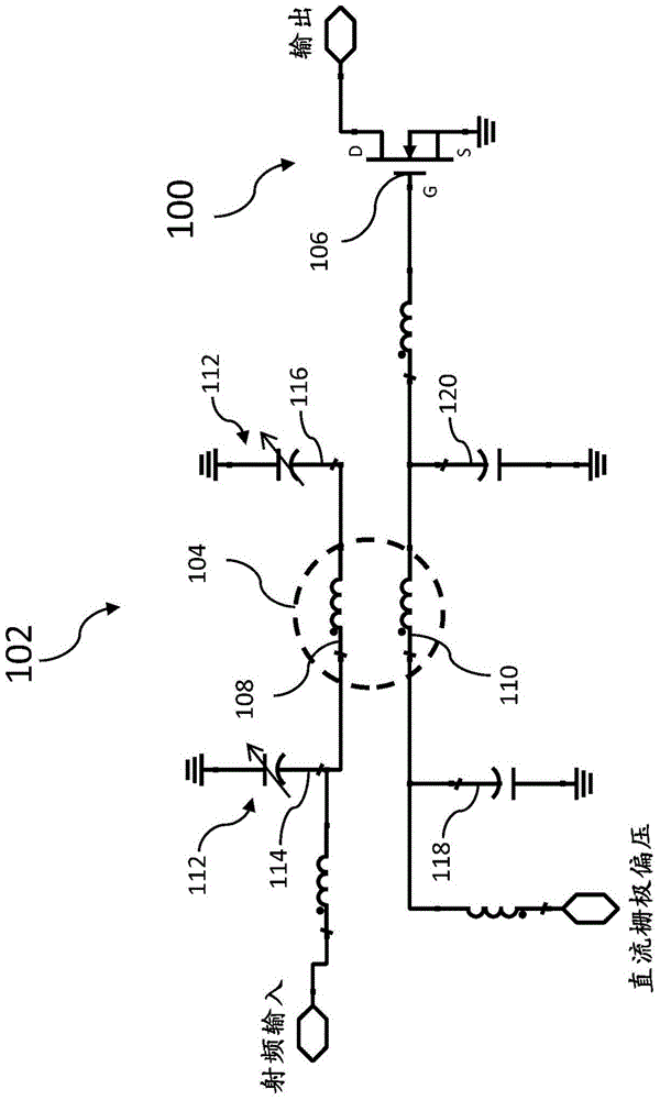
[0015] According to embodiments described herein, the RF power transistor 100 is packaged with an input matching network 102 including a transformer 104 between the RF input leads and the gate 106 of the RF power transistor 100 . Transformer 104 includes primary inductor 108 and secondary inductor 110 that are inductively coupled to each other but physically disconnected. Thus, the transformer 104 blocks DC voltage between the RF input lead and the gate terminal 106 and propagates an AC voltage within a defined frequency range from the RF input lead to the gate terminal 106 .

[0016] The input matching network 102 includes a tuning capacitor 112 electrically connected to the radio frequency input lead and physically disconnected from the gate terminal 106 . That is, tuning capacitor 112 is located on the primary side of transformer 104 . The capacitance of tuning capacitor 112 can be adjusted by varying the DC bias voltage applied to the RF input lead. Therefore, the tuning...


PUM


Abstract

The invention relates to a packaged RF power transistor. The packaged RF power transistor includes an RF input lead, a DC gate bias lead, an RF power transistor comprising gate, source and drain terminals, and an input match network. The input match network includes a primary inductor electrically connected to the RF input lead, a secondary inductor electrically connected to the gate terminal and to the DC gate bias lead, and a tuning capacitor electrically connected to the RF input lead and physically disconnected from the gate terminal. The input match network is configured to block DC voltages between the RF input lead and the gate terminal and to propagate AC voltages in a defined frequency range from the RF input lead to the gate terminal. The tuning capacitor is configured to adjust a capacitance of the input match network based upon a variation in DC voltage applied to the RF input lead.

Description

technical field [0001] This instant application relates to radio frequency power transistors, and more specifically to input matching of radio frequency power transistors. Background technique [0002] High power RF transistors such as LDMOS (Laterally Diffused Metal Oxide Semiconductor) transistors have input and output impedances significantly lower than 50 ohms (high quality factor impedance), however functional RF circuits must be matched to 50 ohms. To facilitate impedance matching to 50 ohms, RF transistors are usually designed with matching circuits on the input and output of the transistor, which are integrated into the packaged transistor. The matching network helps reduce the figure of merit of the packaged transistor to make it easier to match 50 ohms. Typically, impedance improvement can only be achieved in a small frequency range. In addition, matching networks help shape the frequency response of transistors and amplifiers to have high gain at the desired fre...

Claims


Application Information

Patent Timeline
IPC IPC(8): H03F1/56H03H7/38
CPCH03F1/565H03H7/38H03F3/193H03F2200/534H01L2224/49175H01L2223/6655H01L23/66
Inventor M·玛贝尔B·阿加E·哈希莫托
Owner 沃孚半导体公司
Learn More