Semiconductor integrated circuit, latch circuit and flip-flop
A technology of integrated circuits and latch circuits, applied in logic circuits, electrical components, and generating electric pulses, etc., can solve the problems of reduced transistor drive capability, inability to maintain latch signals, and inability to write data signals, etc., to achieve low power consumption volume effect
- Summary
- Abstract
- Description
- Claims
- Application Information
AI Technical Summary
Problems solved by technology
Method used
Image

Examples
Embodiment approach 1
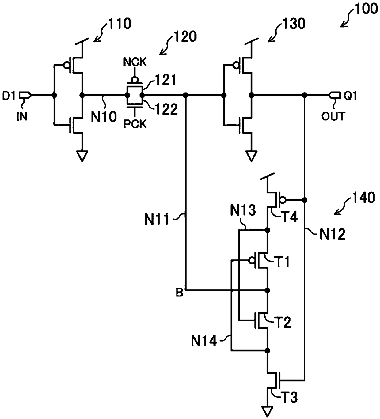
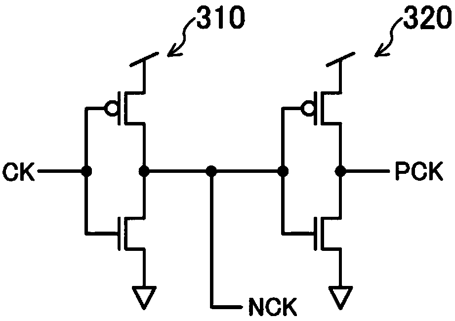
[0032] Figure 1A An example of a circuit diagram of the latch circuit according to Embodiment 1 is shown. Figure 1B It is a conceptual diagram showing a circuit for processing a clock signal in the latch circuit according to the first embodiment.
[0033] like Figure 1A As shown, the latch circuit 100 has: two inverters 110 (first inverter) and an inverter 130 (second inverter) connected in series between the input terminal IN and the output terminal OUT; The control switch 120 between the inverter 110 and the inverter 130; and the latch feedback section 140 (semiconductor integrated circuit), which receives the latch signal Q1 output from the output terminal OUT to generate the latch feedback signal B, and Feedback to the input of inverter 130 . Between the output of the inverter 110 and the input of the control switch 120, the node N10 is connected, between the output of the control switch 120, the input of the inverter 130, and the output of the latch feedback part 140,...
Embodiment approach 2
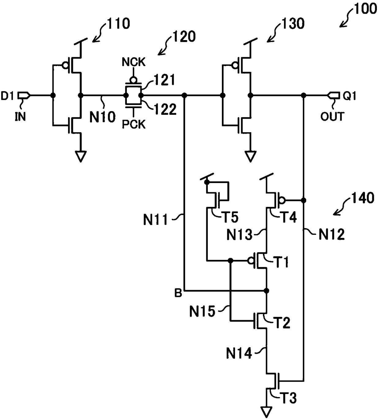
[0046] Figure 2A An example of a circuit diagram of a latch circuit according to Embodiment 2 is shown. exist Figure 2A In addition to the latch feedback section 140, the configuration and Figure 1A same or similar. Figure 2B is a conceptual diagram of a circuit for processing a clock signal in the latch circuit according to Embodiment 2, and shows Figure 1B same circuit.
[0047] like Figure 2A As shown, the latch feedback unit 140 includes: an N-type transistor T5 (the fourth transistor) whose gate and drain are connected to the power supply; a P-type transistor T4 (the first transistor) whose source is connected to the power supply and whose gate is connected to the node N12. ); a P-type transistor T1 (fifth transistor) connected between the node N13 to which the drain of the P-type transistor T4 is connected and the node N11, and whose gate is connected to the source of the N-type transistor T5 via the node N15; N-type transistor T2 (second transistor) whose dra...
Embodiment approach 3
[0055] Figure 3A An example of a circuit diagram of a latch circuit according to Embodiment 3 is shown. exist Figure 3A In, the configuration other than the latch feedback section 140 is the same as Figure 1A same or similar. and, if Figure 3A As shown, the latch feedback section 140 and the Figure 2A Compared with the structure of the above, the connection between the gate of the N-type transistor T2 (second transistor) and the source of the N-type transistor T5 (sixth transistor) is omitted, and a P-type transistor T6 (fourth transistor) is also provided, the gate of which is The electrode and the drain are grounded, and the source is connected to the gate of the N-type transistor T2. Figure 3B is a conceptual diagram of a circuit for processing a clock signal in the latch circuit according to Embodiment 3, and shows Figure 1B same circuit.
[0056] By this composition, with Figure 1A Similarly, the latch function is realized by the latch feedback unit 140 and ...
PUM
 Abstract
Description
Claims
Application Information
 - Generate Ideas
- Intellectual Property
- Life Sciences
- Materials
- Tech Scout
- Unparalleled Data Quality
- Higher Quality Content
- 60% Fewer Hallucinations
Browse by: Latest US Patents, China's latest patents, Technical Efficacy Thesaurus, Application Domain, Technology Topic, Popular Technical Reports.
© 2025 PatSnap. All rights reserved.Legal|Privacy policy|Modern Slavery Act Transparency Statement|Sitemap|About US| Contact US: help@patsnap.com