Inverted Green Quantum Dot Thin Film Electroluminescent Device
An electroluminescent device and quantum dot luminescence technology, which is applied in the direction of electric solid state devices, electrical components, semiconductor devices, etc., can solve the problem of not being able to meet the requirements of hole injection, high hole injection barrier, and difficult hole injection, etc. question
- Summary
- Abstract
- Description
- Claims
- Application Information
AI Technical Summary
Problems solved by technology
Method used
Image
Examples
preparation example Construction
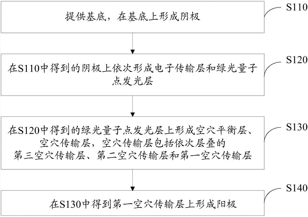
[0051] In addition, the present invention also provides a method for preparing the above-mentioned inverted green light quantum dot thin film electroluminescent device 10, such as image 3 As shown, the method includes the following steps S110-S140.
[0052] S110, providing a substrate, and forming a cathode on the substrate.
[0053] The material of the substrate can be glass, and the substrate can be ultrasonically treated with detergent, acetone, ethanol and isopropanol for 15 minutes each. Then vapor deposition, sputtering, sputtering or electrochemical vapor deposition on the substrate to form the cathode. The material of the cathode can be indium tin oxide (ITO), fluorine-doped tin oxide (FTO), aluminum-doped zinc oxide (AZO), indium-doped zinc oxide (IZO), etc., and the thickness of the cathode is 80nm-200nm.
[0054] Preferably, indium tin oxide (ITO) is sputtered onto the glass substrate by sputtering.
[0055] In this embodiment, after the cathode is formed on the...
Embodiment 1
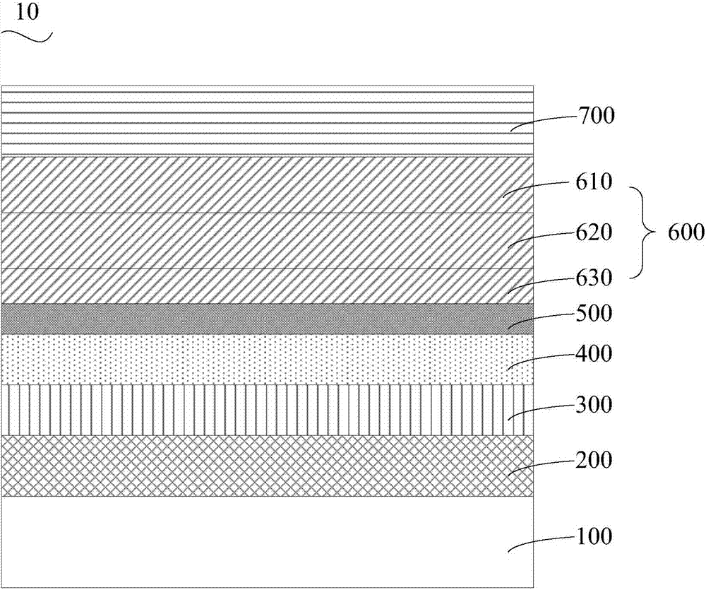
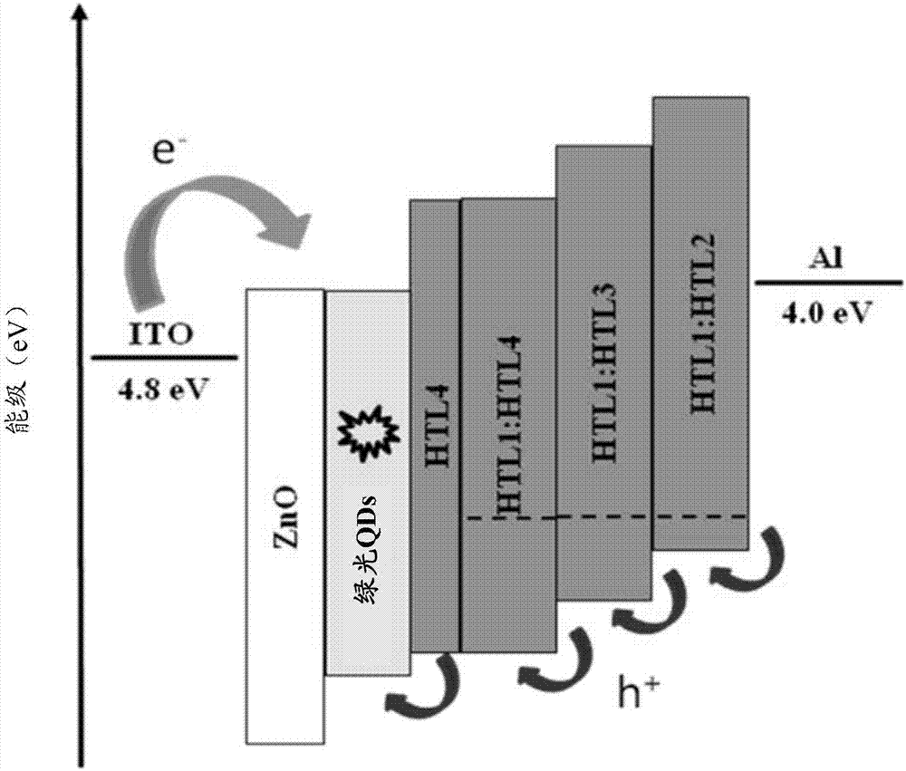
[0067] The structure of the inverted green light quantum dot thin film electroluminescence device is a substrate, a cathode, an electron transport layer, a green light quantum dot light-emitting layer, a hole balance layer, a hole transport layer and an anode. Wherein the hole transport layer comprises a stacked first hole transport layer, a second hole transport layer and a third hole transport layer. The third hole transport layer is in direct contact with the hole transport layer. The thickness of the hole balancing layer is 8 nm, and the material of the hole balancing layer is the fourth hole transport material (HTL4), and HTL4 is 2-hydroxy-3-methyl-2-cyclopenten-1-one (mCP). The thickness of the third hole transport layer is 15nm, and the material of the third hole transport layer is a mixture of the first hole transport material (HTL1) and the fourth hole transport material (HTL4), wherein HTL1 is molybdenum oxide (MoO 3 ), HTL4 is 2-hydroxy-3-methyl-2-cyclopenten-1-one...
Embodiment 2
[0073] The thickness of the hole balance layer in the inverted green light quantum dot thin film electroluminescent device of this embodiment is 5 nm, and the material of the hole balance layer is HTL4, and HTL4 is mCP. The thickness of the third hole transport layer is 10nm, and the material of the third hole transport layer is a mixture of HTL1 and HTL4, wherein HTL1 is MoO 3 , HTL4 for mCP, MoO 3 The mass ratio to mCP is 1:2. The thickness of the second hole transport layer is 11nm, and the material of the second hole transport layer is a mixture of HTL1 and HTL3, wherein HTL1 is MoO 3 , HTL3 for CBP, MoO 3 The mass ratio to CBP is 1:3. The thickness of the first hole transport layer is 20nm, and the material of the first hole transport layer is a mixture of HTL1 and HTL2, wherein HTL1 is MoO 3 , HTL2 for NPB, MoO 3 The mass ratio to NPB is 1:2. All the other are identical with embodiment 1.
[0074] The specific preparation method of the inverted green light quantum...
PUM
 Abstract
Description
Claims
Application Information
 - R&D
- Intellectual Property
- Life Sciences
- Materials
- Tech Scout
- Unparalleled Data Quality
- Higher Quality Content
- 60% Fewer Hallucinations
Browse by: Latest US Patents, China's latest patents, Technical Efficacy Thesaurus, Application Domain, Technology Topic, Popular Technical Reports.
© 2025 PatSnap. All rights reserved.Legal|Privacy policy|Modern Slavery Act Transparency Statement|Sitemap|About US| Contact US: help@patsnap.com


