mobile terminal
A mobile terminal and frame technology, applied in the field of communication, can solve problems such as integrated design of metal frame antenna, poor antenna radio frequency performance, difficult antenna debugging, etc., achieve convenient and flexible debugging, improve utilization rate, and avoid structural modification effect of demand
- Summary
- Abstract
- Description
- Claims
- Application Information
AI Technical Summary
Problems solved by technology
Method used
Image
Examples
Embodiment 1
[0067] Such as Figure 16 As shown, this example is for a metal-frame mobile terminal with a "5.5-inch screen, MIC and USB placed in the clear area of the antenna". The antenna structure is as follows: Figure 4 Based on the scheme shown, only the MIC and USB grounding areas are introduced. The basic information of other models is as follows:
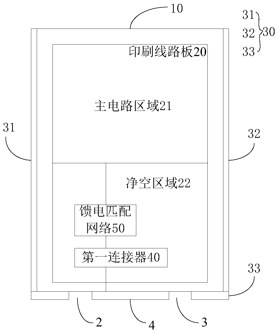
[0068] The length, width and height of the square area formed by the metal frame are (147mm*76mm*5.5mm). In order to simulate the influence of the plastic shell of the actual mobile phone, a plastic material with a thickness of 1mm is set on the upper and lower spaces of the square area (dielectric constant 2.7, loss angle Tangent 0.03@10GHz), the length of the middle metal frame 4 is 48mm, and the width of the slots 2 and 3 is 0.8mm.
[0069] The PWB clearance area 22 is 8 mm in the length direction of the mobile phone.
[0070] The selected inductor and capacitor values are 2nH for L3, 9nH for L4, 4nH for L5, 1.6pF for C1, 1.2pF...
Embodiment 2
[0073] Such as Figure 19 As shown, this example is for a metal-frame mobile phone with a "4.4-inch screen, only the MIC is placed in the clear area of the antenna". The antenna structure is as follows: Figure 4 On the basis of the scheme shown, there are the following changes:
[0074] Because the set frame size basically meets the requirements, L1 and L2 for auxiliary fine-tuning of the electrical size of the metal frame are omitted.
[0075] At the same time, because the USB is not placed in the antenna clearance area and the size of the clearance area is reasonable, the first resistor R1 for balancing the low-frequency impedance mismatch and radiation efficiency of the antenna is also omitted.
[0076] In addition, in the feeding matching network 50, a coupling capacitor "first capacitor C1" formed by a gap between a suspended wire at the end and the metal frame 4 and the first connector 40 is used to replace the Figure 5 The first capacitor C1 in the fast matching n...
PUM
 Abstract
Description
Claims
Application Information
 - R&D
- Intellectual Property
- Life Sciences
- Materials
- Tech Scout
- Unparalleled Data Quality
- Higher Quality Content
- 60% Fewer Hallucinations
Browse by: Latest US Patents, China's latest patents, Technical Efficacy Thesaurus, Application Domain, Technology Topic, Popular Technical Reports.
© 2025 PatSnap. All rights reserved.Legal|Privacy policy|Modern Slavery Act Transparency Statement|Sitemap|About US| Contact US: help@patsnap.com


