Lead frame handling system for semiconductor packaging systems
A lead frame and packaging system technology, applied in the field of semiconductor packaging clamping, can solve the problems of difficult product grasping, gold wire breakage, lead frame deformation, etc., and achieve the effects of fast clamping, convenient energy, and timely action
- Summary
- Abstract
- Description
- Claims
- Application Information
AI Technical Summary
Problems solved by technology
Method used
Image
Examples
Embodiment Construction
[0013] Below in conjunction with accompanying drawing, by describing embodiment, the present invention will be further described:
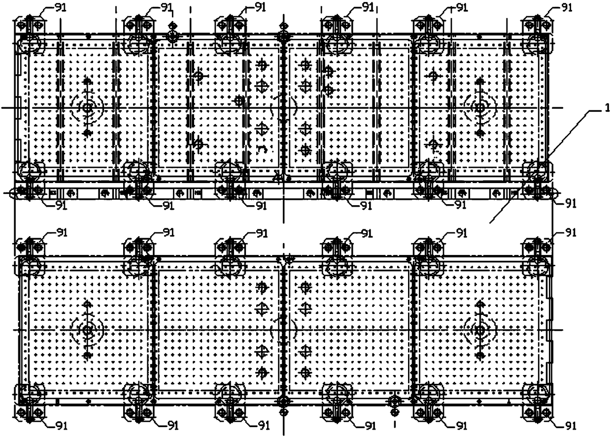
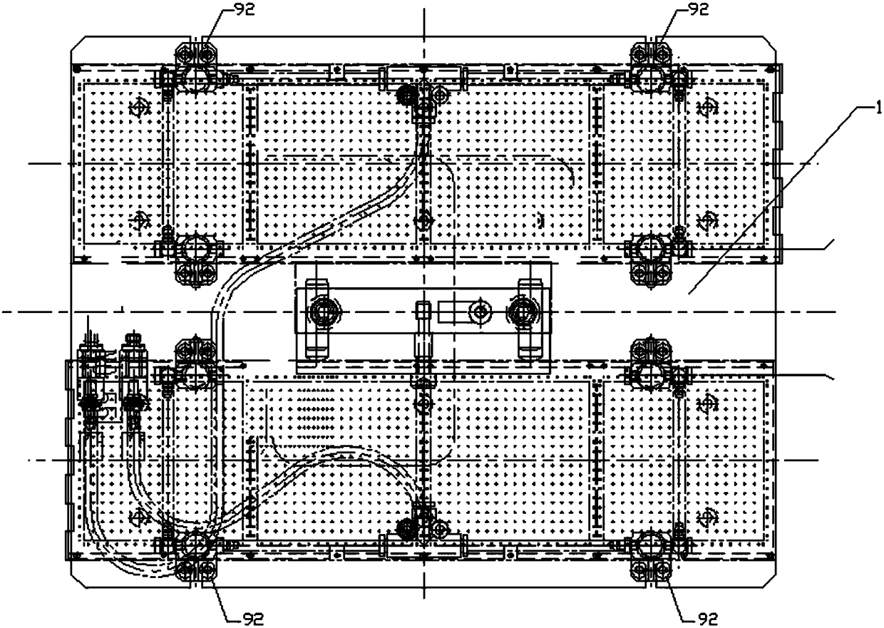
[0014] Such as Figures 1 to 4 As shown, a lead frame clamping system for a semiconductor packaging system of the present invention includes a clamping system and a guide rail pair (not shown in the figure), the guide rail pair includes a vertical guide rail and a horizontal guide rail, and the clamping system is arranged on the guide rail pair and can move along the guide rail pair. The clamping system includes a material loading and clamping device and a material taking and clamping device. The initial position of the loading and picking device is located above the semiconductor lead frame 1 before packaging, and the material picking and picking device is arranged above the semiconductor lead frame 1 after packaging.
[0015] The feeding and gripping device includes 12 pairs of pneumatic manipulators I91, the pneumatic manipulator I91 includes ...
PUM
 Abstract
Description
Claims
Application Information
 - R&D
- Intellectual Property
- Life Sciences
- Materials
- Tech Scout
- Unparalleled Data Quality
- Higher Quality Content
- 60% Fewer Hallucinations
Browse by: Latest US Patents, China's latest patents, Technical Efficacy Thesaurus, Application Domain, Technology Topic, Popular Technical Reports.
© 2025 PatSnap. All rights reserved.Legal|Privacy policy|Modern Slavery Act Transparency Statement|Sitemap|About US| Contact US: help@patsnap.com


