
LED chip structure capable of increasing light-emitting area and manufacturing method

A technology of LED chip and light-emitting area, applied in electrical components, circuits, semiconductor devices, etc., can solve the problems of loss of light-emitting area and further improvement of light-emitting efficiency, and achieve the effect of chip voltage optimization

Active Publication Date: 2016-06-08
XIAMEN CHANGELIGHT CO LTD
View PDF6 Cites 2 Cited by
  • Summary
  • Abstract
  • Description
  • Claims
  • Application Information

AI Technical Summary

Problems solved by technology

The N electrode pad is directly formed on the P-GaN and passivation layer, although the loss of the light emitting area can be partially reduced, however, the N electrode is in contact with the N-GaN plane at the same time, and part of the light emitting area is still lost, and the luminous efficiency needs to be further improved. improve

Method used


Image

  • LED chip structure capable of increasing light-emitting area and manufacturing method
  • LED chip structure capable of increasing light-emitting area and manufacturing method
  • LED chip structure capable of increasing light-emitting area and manufacturing method

Examples


Embodiment Construction

[0046] The present invention will be described in detail below in conjunction with the accompanying drawings and specific embodiments.

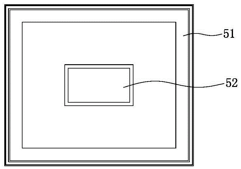
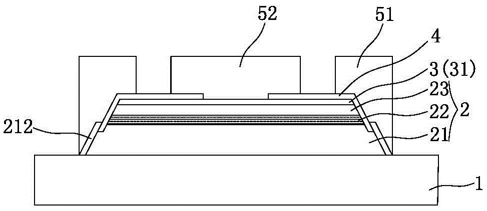
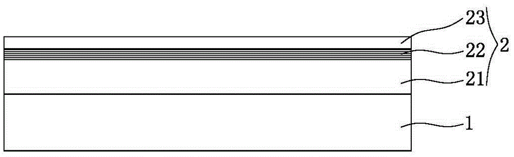
[0047] refer to Figures 1 to 3f As shown, Embodiment 1 of an LED chip structure with increased light-emitting area disclosed in the present invention includes a substrate 1 , an epitaxial layer 2 , a conductive layer 3 , an insulating layer 4 , an N electrode 51 and a P electrode 52 .

[0048] The epitaxial layer 2 is composed of N-GaN 21 , active light emitting layer 22 and P-GaN 23 formed in sequence, and the N-GaN 21 is formed on the substrate 1 . The conductive layer 3 is formed on the P-GaN23, and the P electrode 52 is formed on the conductive layer 3; in this embodiment, the conductive layer 3 is a metal reflective layer 31, forming a flip chip. The metal reflective layer 31 is made of silver, titanium, aluminum, chromium, indium, tin, gold and alloys thereof, and is arranged in a single-layer or multi-layer structure.

[0049] A fir...


PUM


Abstract

The invention discloses an LED chip structure capable of increasing the light-emitting area. The LED chip structure comprises a substrate, an epitaxial layer, a conducting layer, a P electrode and an N electrode. The epitaxial layer is composed of N-GaN, an active light-emitting layer and P-GaN which are formed in sequence, and N-GaN is formed on the substrate. The conducting layer is formed on P-GaN, and the P electrode is formed on the conducting layer. A first slope is formed on the outer side walls of the active light-emitting layer and P-GaN, an insulating layer is formed on the first slope, and part of the insulating layer extends to the surface of the conducting layer. A second slope is formed on the outer side wall of N-GaN, and the N electrode is formed on the second slope and insulated from the active light-emitting layer, P-GaN and the conducting layer through the insulating layer. The invention further discloses a manufacturing method of the LED chip structure capable of increasing the light-emitting area. The LED chip structure can further reduce the light-emitting area loss and improve the light-emitting efficiency, and thus the area of a light-emitting layer of a chip is increased under the same chip area.

Description

technical field [0001] The invention relates to the technical field of LEDs, in particular to an LED chip structure with increased light-emitting area and a manufacturing method. Background technique [0002] In the prior art, GaN-based light emitting diode structures are divided into front-mount structure, vertical structure and front-mount structure. Among them, the front-mounted structure chip exposes the N-type GaN layer by dry etching, then forms a transparent conductive layer on the P-type GaN, and finally uses metals such as nickel and gold to make P / N electrodes to form a current path to emit light; vertical The structural chip forms a conductive bottom layer by using conductive sinking or substrate transfer, so that the P / N electrodes are respectively located on the upper and lower sides of the chip; the manufacturing process of the flip-chip structure chip is similar to that of the front chip, except that the transparent conductive layer is formed by the reflective...

Claims


Application Information

Patent Timeline
IPC IPC(8): H01L33/20H01L33/40H01L33/00
CPCH01L33/0075H01L33/20H01L33/405H01L33/42
Inventor 邬新根李俊贤陈亮陈凯轩张永刘英策周弘毅魏振东
Owner XIAMEN CHANGELIGHT CO LTD
Learn More