PCB manufacturing method
A manufacturing method and technology of inner layer core board, applied in the direction of printed circuit manufacturing, printed circuit connected with non-printed electrical components, electrical components, etc. Problems such as signal loss, to improve the quality and speed of signal transmission, and to expand the use of the effect
- Summary
- Abstract
- Description
- Claims
- Application Information
AI Technical Summary
Problems solved by technology
Method used
Image

Examples
Embodiment 1
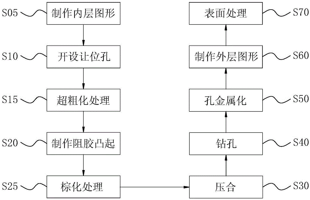
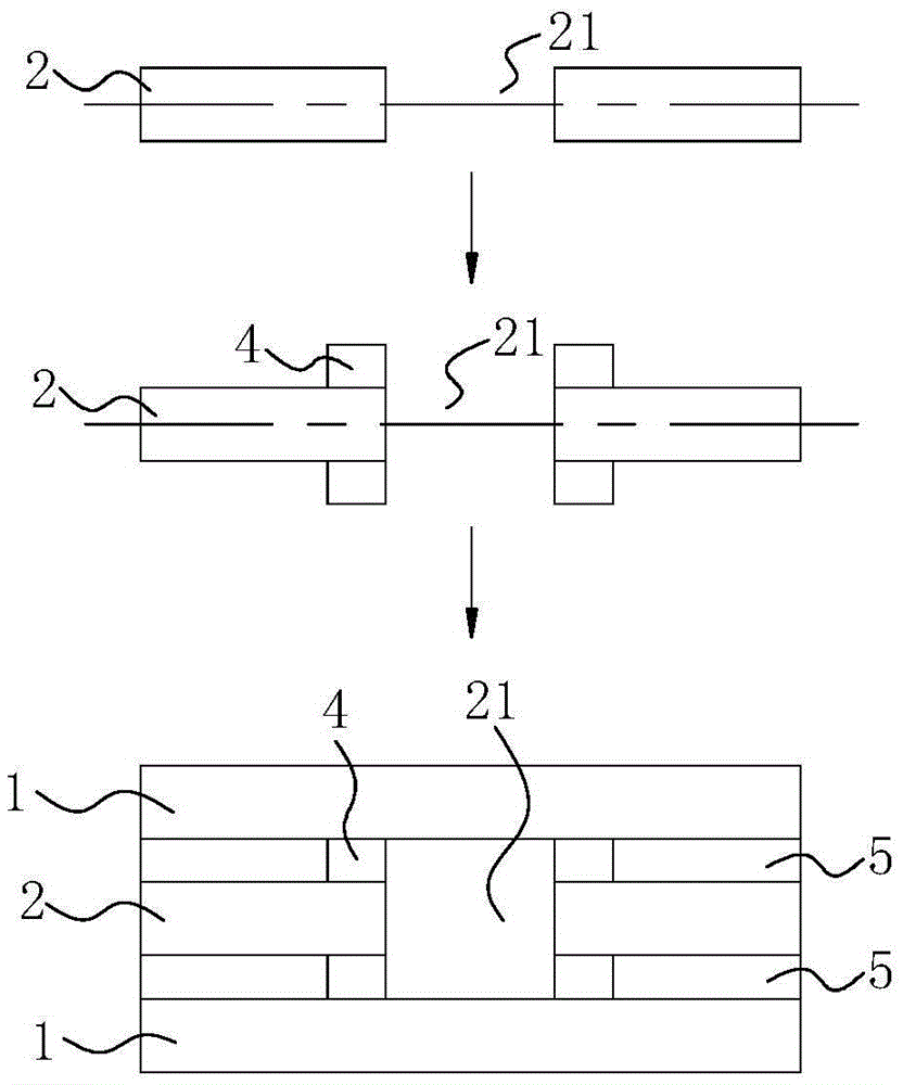
[0068] Such as figure 1 and figure 2 Shown, a kind of manufacturing method of PCB comprises the following steps:
[0069] S05, making the inner layer graphics on the inner layer core board;
[0070] S10. Provide the inner core board 2 that needs to be drilled, and set up a relief hole 21 on the inner core board 2 that needs to be drilled;
[0071] S15, performing super-roughening treatment on the inner core board;
[0072] S20, on the end surface of the inner layer core board 2 to be opened and on the edge of the relief hole 21, make a glue-resisting protrusion 4;
[0073] S25, browning the inner core board;
[0074] S30, providing a non-perforated core board and a prepreg 5, and pressing the non-perforated core board, the prepreg 5 and the inner core board 2 to be perforated to form a laminated board with a closed cavity;
[0075] S40, drilling the plywood, and performing post-drilling treatment;
[0076] S50, performing electroless copper deposition and electroplating...
Embodiment 2
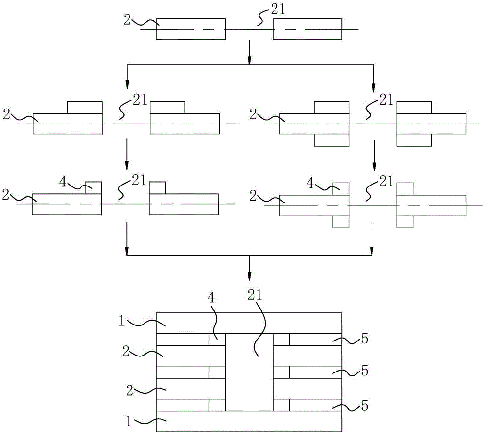
[0093] Such as figure 1 and image 3 Shown, a kind of manufacturing method of PCB comprises the following steps:
[0094] S05, making the inner layer graphics on the inner layer core board;
[0095] S10. Provide the inner core board 2 that needs to be drilled, and set up a relief hole 21 on the inner core board 2 that needs to be drilled;
[0096] S15, performing super-roughening treatment on the inner core board;
[0097] S20, on the end surface of the inner layer core board 2 to be opened and on the edge of the relief hole 21, make a glue-resisting protrusion 4;
[0098] S25, browning the inner core board;
[0099] S30, providing a non-perforated core board and a prepreg 5, and pressing the non-perforated core board, the prepreg 5 and the inner core board 2 to be perforated to form a laminated board with a closed cavity;
[0100] S40, drilling the plywood, and performing post-drilling treatment;
[0101] S50, performing electroless copper deposition and electroplating ...
Embodiment 3
[0120] Such as figure 1 and Figure 4 Shown, a kind of manufacturing method of PCB comprises the following steps:
[0121] S05, making the inner layer graphics on the inner layer core board;
[0122] S10. Provide the inner core board 2 that needs to be drilled, and set up a relief hole 21 on the inner core board 2 that needs to be drilled;
[0123] S15, performing super-roughening treatment on the inner core board;
[0124] S20, on the end surface of the inner layer core board 2 to be opened and on the edge of the relief hole 21, make a glue-resisting protrusion 4;
[0125] S25, browning the inner core board;
[0126] S30, providing a non-perforated core board and a prepreg 5, and pressing the non-perforated core board, the prepreg 5 and the inner core board 2 to be perforated to form a laminated board with a closed cavity;
[0127] S40, drilling the plywood, and performing post-drilling treatment;
[0128] S50, performing electroless copper deposition and electroplating...
PUM
 Abstract
Description
Claims
Application Information
 - Generate Ideas
- Intellectual Property
- Life Sciences
- Materials
- Tech Scout
- Unparalleled Data Quality
- Higher Quality Content
- 60% Fewer Hallucinations
Browse by: Latest US Patents, China's latest patents, Technical Efficacy Thesaurus, Application Domain, Technology Topic, Popular Technical Reports.
© 2025 PatSnap. All rights reserved.Legal|Privacy policy|Modern Slavery Act Transparency Statement|Sitemap|About US| Contact US: help@patsnap.com