Array substrate and preparation method thereof, display panel and display device
A technology for array substrates and substrate substrates, applied in semiconductor/solid-state device manufacturing, optics, instruments, etc., can solve problems such as air bubbles and display panel gaps, avoid film gaps, avoid air bubbles, and improve high temperature and high humidity resistance Effect
- Summary
- Abstract
- Description
- Claims
- Application Information
AI Technical Summary
Problems solved by technology
Method used
Image


Examples
Embodiment 1
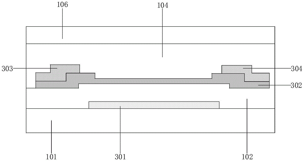
[0043] figure 1 It is a schematic structural diagram of an array substrate provided in Embodiment 1 of the present invention. Such as figure 1 As shown, the array substrate includes a base substrate 101, the base substrate 101 includes a display area and a sealant coating area, the base substrate 101 is provided with a thin film transistor and an organic material layer 104, the organic The material layer 104 is disposed on the display area and the sealant coating area, and the organic material layer 104 located in the sealant coating area is provided with a thermal conduction layer 105 on the first surface away from the base substrate 101 . Optionally, a passivation layer 106 is disposed above the organic material layer 104 . The thermal conduction layer 105 is used to conduct heat, reducing the degree of thermal expansion of the organic material, thereby preventing the expansion of the organic material from affecting the junction force between the organic material layer, th...
Embodiment 2
[0048] image 3 It is a schematic structural diagram of an array substrate provided in Embodiment 2 of the present invention. Such as image 3As shown, the array substrate includes a base substrate 101, the base substrate 101 includes a display area and a sealant coating area, the base substrate 101 is provided with a thin film transistor and an organic material layer 104, the organic The material layer 104 is disposed on the display area and the sealant coating area, and the organic material layer 104 located in the sealant coating area is provided with a heat conduction layer 105 on the second surface close to the base substrate 101 . Optionally, a passivation layer 106 is disposed above the organic material layer 104 . The thermal conduction layer 105 is used to conduct heat, reducing the degree of thermal expansion of the organic material, thereby preventing the expansion of the organic material from affecting the junction force between the organic material layer, the ga...
Embodiment 3
[0053] Figure 4 It is a schematic structural diagram of an array substrate provided in Embodiment 3 of the present invention. Such as Figure 4 As shown, the array substrate includes a base substrate 101, the base substrate 101 includes a display area and a sealant coating area, the base substrate 101 is provided with a thin film transistor and an organic material layer 104, the organic The material layer 104 is disposed on the display area and the sealant coating area, and the organic material layer 104 located in the sealant coating area is away from the first surface of the base substrate 101 and close to the first surface of the base substrate 101. The two surfaces are provided with a heat conducting layer 105 . Optionally, a passivation layer 106 is disposed above the organic material layer 104 . The thermal conduction layer 105 is used to conduct heat, reducing the degree of thermal expansion of the organic material, thereby preventing the expansion of the organic ma...
PUM
 Abstract
Description
Claims
Application Information
 - R&D
- Intellectual Property
- Life Sciences
- Materials
- Tech Scout
- Unparalleled Data Quality
- Higher Quality Content
- 60% Fewer Hallucinations
Browse by: Latest US Patents, China's latest patents, Technical Efficacy Thesaurus, Application Domain, Technology Topic, Popular Technical Reports.
© 2025 PatSnap. All rights reserved.Legal|Privacy policy|Modern Slavery Act Transparency Statement|Sitemap|About US| Contact US: help@patsnap.com