Shift register, gate drive circuit and display panel

A shift register and gate technology, which is applied in static memory, digital memory information, instruments, etc., can solve the problem of increased power consumption of shift registers

Active Publication Date: 2016-05-04
BOE TECH GRP CO LTD +1
View PDF6 Cites 16 Cited by
  • Summary
  • Abstract
  • Description
  • Claims
  • Application Information

AI Technical Summary

Problems solved by technology

[0004] Embodiments of the present invention provide a shift register, a gate drive circuit, and a display panel, which are used to solve the problem of frequent switching between high and low potentials and the existence of output transistors when the clock signal terminal is used as the power supply terminal of the drive signal output terminal in the prior art. The coupling effect of the parasitic capacitance leads to the problem of increased power consumption of the shift register

Method used


Image

  • Shift register, gate drive circuit and display panel
  • Shift register, gate drive circuit and display panel
  • Shift register, gate drive circuit and display panel

Examples


Embodiment 1

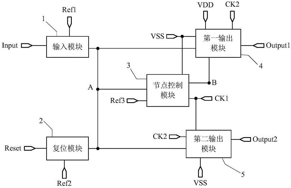
[0106] by Figure 3a The structure of the shift register shown is taken as an example to describe its working process, wherein, in Figure 3a In the shift register shown, all the switch transistors are N-type switch transistors; the potential of the first reference signal terminal Ref1 is high potential, and the potential of the second reference signal terminal Ref2 is low potential; the potential of the first DC signal terminal VSS The signal is low potential, and the signal of the second DC signal terminal VDD is high potential; the corresponding input and output timing diagram is as follows Figure 5a shown. Specifically, choose the Figure 5a There are five stages in the shown input-output timing diagram, the first stage T1 , the second stage T2 , the third stage T3 , the fourth stage T4 and the fifth stage T5 .

[0107] In the first phase T1, Input=1, Reset=0, CK1=0, CK2=1.

[0108] Since Reset=0, the second switching transistor M2 is turned off; because CK1=0, the th...

Embodiment 2

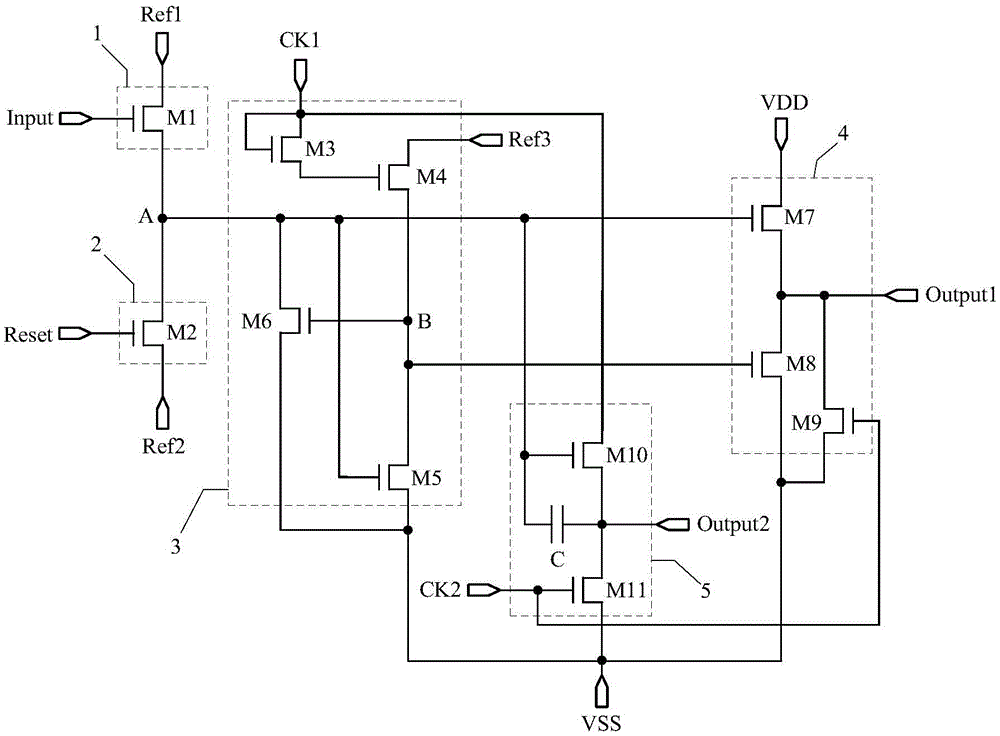
[0119] by Figure 4a The structure of the shift register shown is taken as an example to describe its working process, wherein, in Figure 4a In the shift register shown, all the switch transistors are N-type switch transistors, and each N-type switch transistor is turned on under the action of a high potential, and is turned off under the action of a low potential; the potential of the first reference signal terminal Ref1 is a high potential, The potential of the second reference signal terminal Ref2 is low potential; the signal of the first DC signal terminal VSS is low potential, and the signal of the second DC signal terminal VDD is high potential. The corresponding input and output timing diagrams are as follows Figure 7a shown. Specifically, choose the Figure 7a There are five stages in the shown input-output timing diagram, the first stage T1 , the second stage T2 , the third stage T3 , the fourth stage T4 and the fifth stage T5 .

[0120] In the first phase T1, In...


PUM


Abstract

The invention discloses a shift register, a gate drive circuit and a display panel. The shift register comprises an input module, a rest module, a node control module, a first output module and a second output module. A first direct current signal end and a second direct current signal end are taken as power ends of a drive signal output end, so that compared with an existing shift register adopting a clock signal end as a drive signal output end, the power consumption of the shift register can be reduced, and the output stability of the drive signal output end can be improved.

Description

technical field [0001] The invention relates to the field of display technology, in particular to a shift register, a gate drive circuit and a display panel. Background technique [0002] With the rapid development of display technology, the display panel is more and more developed towards the direction of high integration and low cost. Among them, the array substrate line drive (GateDriveronArray, GOA) technology integrates the thin film transistor (ThinFilmTransistor, TFT) gate switch circuit on the array substrate of the display panel to form a scan drive for the display panel, so that the gate integrated circuit ( Integrated Circuit (IC) bonding (Bonding) area and fan-out (Fan-out) area wiring space can not only reduce product cost in terms of material cost and manufacturing process, but also make the display panel symmetrical on both sides and narrow frame In addition, this integration process can also save the Bonding process in the direction of the gate scanning line...

Claims


Application Information

Patent Timeline
Patent Type & Authority Applications(China)
IPC IPC(8): G09G3/20G11C19/28
CPCG09G3/20G11C19/28
Inventor 李金钰
Owner BOE TECH GRP CO LTD
Why Eureka
Try Eureka