
Time sequence correction method and electronic device

An electronic device and timing technology, applied in the fields of electrical digital data processing, CAD circuit design, special data processing applications, etc., can solve the problems of prolonging the chip design cycle, increasing the chip design cost, and increasing the chip power consumption.

Active Publication Date: 2016-04-13
上海兆芯集成电路股份有限公司
View PDF4 Cites 10 Cited by
  • Summary
  • Abstract
  • Description
  • Claims
  • Application Information

AI Technical Summary

Problems solved by technology

However, not every component that violates the design rules is a timing violation, and some even have no timing checks
Therefore, the above method will lead to the insertion of a large number of redundant components, thus increasing the power consumption of the chip, and even the design of some components with dense distribution will lead to deterioration of timing, prolong the chip design cycle, and increase the cost of chip design

Method used

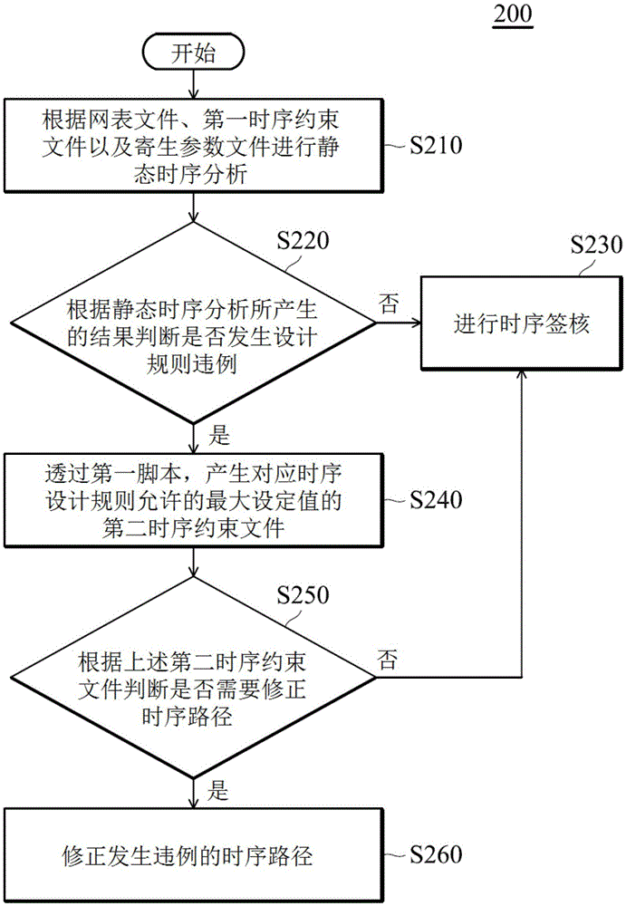
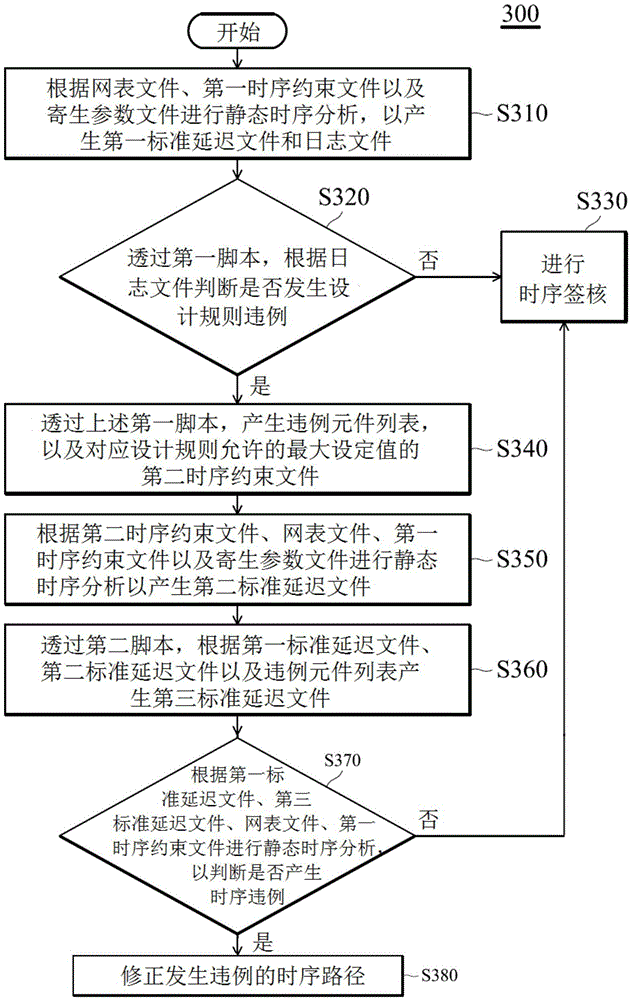

Image

  • Time sequence correction method and electronic device
  • Time sequence correction method and electronic device
  • Time sequence correction method and electronic device

Examples


Embodiment Construction

[0023] What is described in this chapter is the best way to implement the present invention. The purpose is to illustrate the spirit of the present invention rather than to limit the protection scope of the present invention. The protection scope of the present invention should be defined by the claims.

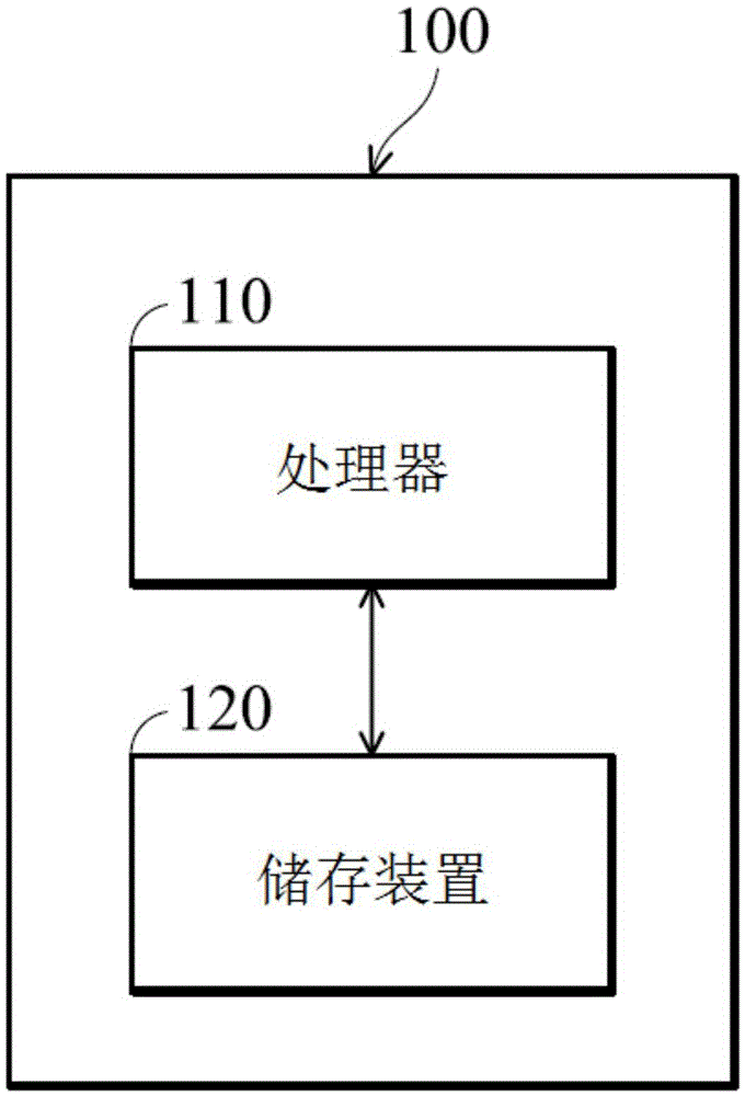
[0024] figure 1 It is a block diagram showing the electronic device 100 according to an embodiment of the present invention. The electronic device 100 is suitable for Electronic Design Automation (EDA) tools and simulation tools for integrated circuit design. The electronic device 100 can simulate circuit operation through electronic design automation (EDA) tools. Such as figure 1 As shown, the electronic device 100 includes a processor 110 and a storage device 120 . exist figure 1 The block diagram in the figure is only for the convenience of describing the embodiment of the present invention, but the present invention is not limited thereto.

[0025] According to an em...


PUM


Abstract

The invention provides a time sequence correction method. The method comprises the following steps: performing static timing analysis according to a netlist file, a first timing constraint file and a parasitic parameter file, so as to generate a first standard delay file and a log file; judging whether design rule violations occur through a first script and according to the log file; when judging that the design rule violations occur, generating a violation component list, and a second timing constraint file of a maximum set value allowed by a corresponding design rule through the first script; and judging whether to correct a timing path according to the second timing constraint file.

Description

technical field [0001] This manual mainly relates to the technique of timing correction, and in particular to the technique of correcting only the timing path where a violation occurs through a designed script. Background technique [0002] In the chip design process, in order to ensure that the actually produced chip can work normally in various environments (that is, the sequence meets the requirements), the chip designer will use the static timing analysis tool (StaticTimingAnalysistool, STAtool) and the process provided by the factory. File (processfile) to simulate the timing information of the design in different environments, and then evaluate whether the design meets the timing requirements. [0003] In order to ensure the timing consistency of design and manufacturing, chip manufacturers will provide chip designers with relevant design rules (such as the maximum signal conversion time), which describe the process boundary conditions (boundary conditions) of electric...

Claims


Application Information

Patent Timeline
IPC IPC(8): G06F17/50
CPCG06F30/33G06F30/398
Inventor 辛玲李冰林哲民李翊
Owner 上海兆芯集成电路股份有限公司
Learn More