A kind of preparation method of ge‑sb‑se chalcogenide nanowire
A nanowire, ge-sb-se technology, applied in the field of nanomaterials, can solve the problems of undisclosed Ge-Sb-Se chalcogenide nanowires, and achieve wide optical transmission range, high linear and nonlinear refractive index, The effect of good thermal stability
- Summary
- Abstract
- Description
- Claims
- Application Information
AI Technical Summary
Problems solved by technology
Method used
Image
Examples
Embodiment 1
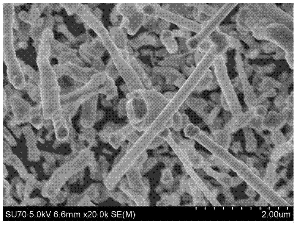
[0030] Weigh Ge 20 Sb 15 Se 65 Put 0.4g of raw material into a quartz crucible, place the crucible in the high temperature zone of a horizontal tube furnace, and place the gold-plated silicon wafer in the low temperature zone, the distance between the high temperature zone and the low temperature zone is 15cm, and vacuumize the furnace , when the pressure reaches 3×10 -2 Start argon at torr, set the flow rate of argon to 100 sccm, and start heating after 10 minutes of argon, in which the temperature in the high temperature zone is set to 500°C, and the temperature in the low temperature zone is set to 400°C, keep at this temperature for 120 minutes, the pressure in the tube remains At 2 torr, after the deposition is over, let the furnace cool down naturally, and take out the grown nanowires when the temperature drops to 70°C. The above substrate is SiO 2 / Si(100) substrate. The Ge-Sb-Se material in the high temperature zone is in the upstream of the gas flow, and the gold...
Embodiment 2
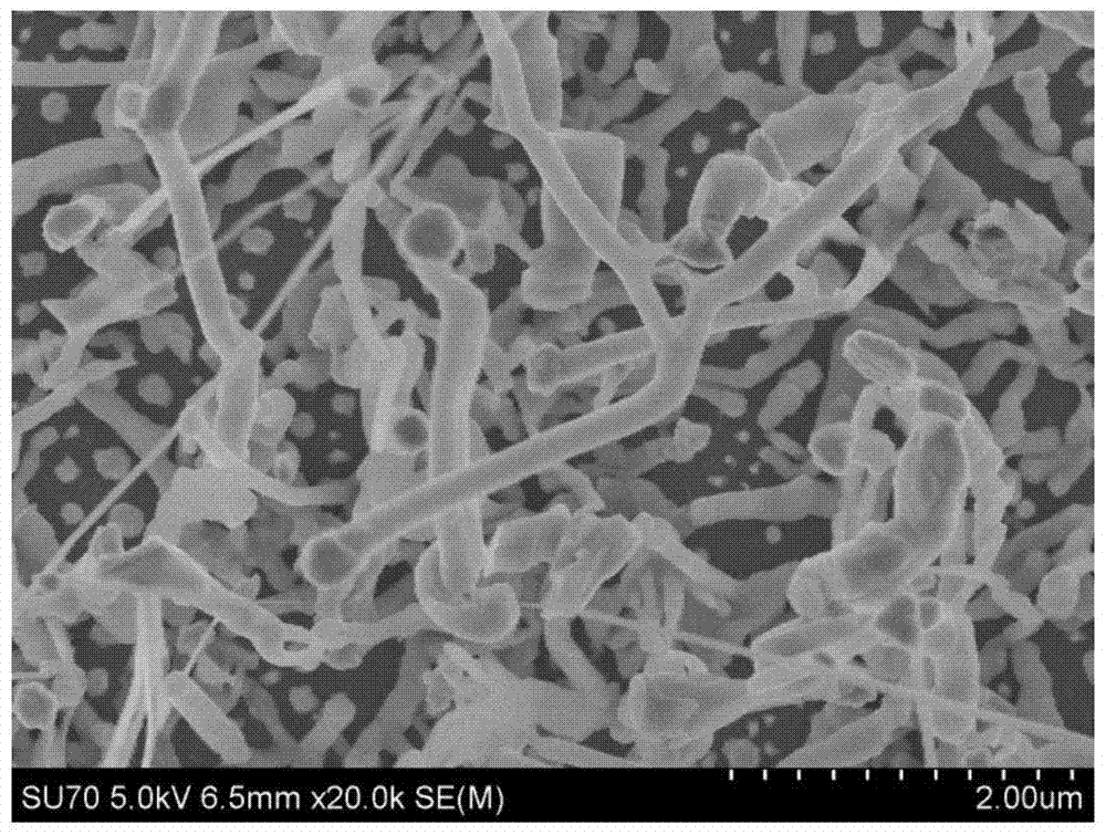
[0033] Same as Example 1, the difference lies in that the temperature in the low temperature zone is set to 350°C. Test the growth status of the Ge-Sb-Se nanowires prepared in the above-mentioned embodiment 2, the test results obtained refer to figure 2 .
Embodiment 3
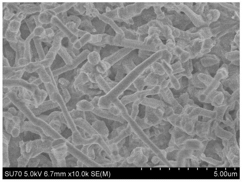
[0035] Same as Example 1, the difference lies in that the temperature in the low temperature zone is set to 300°C. Test the growth status of the Ge-Sb-Se nanowires prepared in the above-mentioned embodiment 3, the test results obtained refer to image 3 .
PUM
| Property | Measurement | Unit |
|---|---|---|
| thickness | aaaaa | aaaaa |
| diameter | aaaaa | aaaaa |
| length | aaaaa | aaaaa |
Abstract
Description
Claims
Application Information
 - R&D Engineer
- R&D Manager
- IP Professional
- Industry Leading Data Capabilities
- Powerful AI technology
- Patent DNA Extraction
Browse by: Latest US Patents, China's latest patents, Technical Efficacy Thesaurus, Application Domain, Technology Topic, Popular Technical Reports.
© 2024 PatSnap. All rights reserved.Legal|Privacy policy|Modern Slavery Act Transparency Statement|Sitemap|About US| Contact US: help@patsnap.com


