A kind of driving thin film transistor and its preparation method

A thin-film transistor and semiconductor technology, applied in transistors, semiconductor/solid-state device manufacturing, semiconductor devices, etc., can solve the problems of reducing Ion, uneven carrier mobility, and pixel period pitch reduction, etc., to reduce the turn-on current Ion , to meet the high PPI pixel drive requirements, reduce the effect of operating current

Active Publication Date: 2018-09-28
KUNSHAN GO VISIONOX OPTO ELECTRONICS CO LTD
View PDF4 Cites 0 Cited by
  • Summary
  • Abstract
  • Description
  • Claims
  • Application Information

AI Technical Summary

Problems solved by technology

[0002] In AMOLED, as the PPI of the pixel increases, the working current required by the pixel decreases, so the turn-on current Ion of the required driving thin film transistor DTFT decreases, and at the same time, the characteristics of the driving thin film transistor STFT still need to maintain a fast charging rate, so It is difficult to meet the above requirements at the same time through one photolithography
In addition, in the layout design of the pixel, due to the increase of the pixel PPI, the pixel period pitch decreases, and the length L of the carrier transmission channel increases relative to the width W, which in turn increases the W / L. Driving thin film transistor DTFT Ion decreases
In terms of process conditions, if the width W of the carrier transmission channel is reduced, the number of polysilicon grains in the direction of the width W of the carrier transmission channel of the driving thin film transistor DTFT will decrease, resulting in uneven carrier mobility, so it is also difficult Reduce Ion by reducing W

Method used


Image

  • A kind of driving thin film transistor and its preparation method
  • A kind of driving thin film transistor and its preparation method
  • A kind of driving thin film transistor and its preparation method

Examples


Embodiment 1

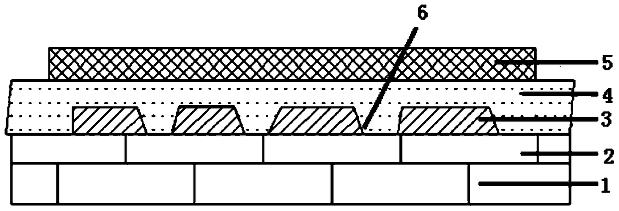
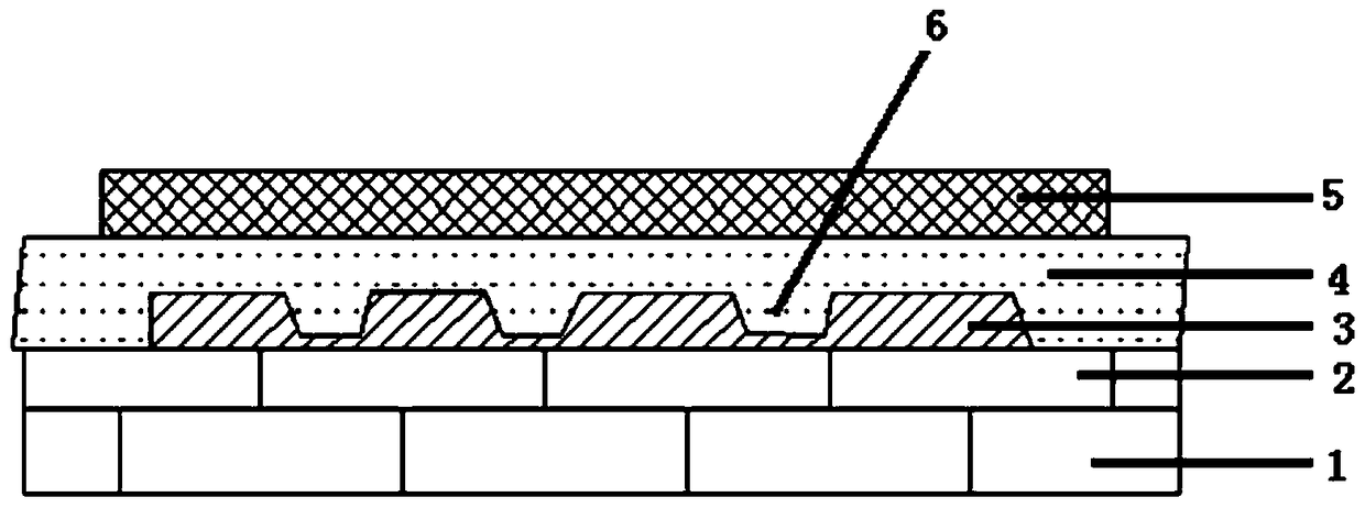
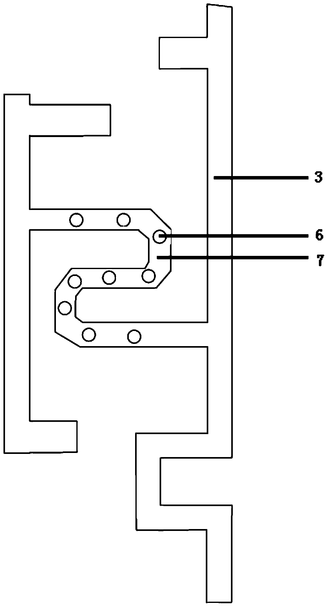
[0037] Such as figure 1 , figure 2 and image 3 As shown, several micropores 6 are arranged in the carrier transport channel 7, and the micropores 6 can hinder the transport of carriers. The centerline of the microhole 6 is perpendicular to the semiconductor layer 3 . Specifically, the centerline is defined as follows: image 3 The cross-sectional shape of the micropore 6 shown in is circular, and the straight line passing through the center of the circular section is the centerline of the micropore 6 . The height of the microhole 6 is less than or equal to the thickness of the semiconductor layer 3 . in figure 1 The height of the microhole 6 in the shown structure is equal to the thickness of the semiconductor layer 3, the figure 2 The height of the microholes 6 is smaller than the thickness of the semiconductor layer 3 . The cross-section of the microhole 6 can be a regular or irregular shape such as a circle, an ellipse, a triangle, and a pentagon. The micropores ...

Embodiment 2

[0039] Such as image 3 and Figure 4 As shown, the carrier transmission channel 7 of the driving thin film transistor of the present invention adopts an irregular sidewall structure, which is used to hinder the transmission of carriers. Specifically, the cross-section of the irregular side wall structure of the carrier transport channel 7 is zigzag or formed by sequentially connecting several arc-shaped structures, or a combination of regular and irregular shapes, the irregular The sidewall constitutes the carrier transport blocking structure. in Figure 4 The cross-section of the irregular side wall structure of the carrier transport channel 7 in the shown structure is formed by sequential connection of zigzag structures. Figure 5 The cross-section of the irregular side wall structure of the carrier transport channel 7 in the shown structure is formed by sequentially connecting several arc-shaped structures. In this embodiment, the sidewall of the carrier transmission c...


PUM


Abstract

The invention provides a drive thin-film transistor and a preparation method thereof. The drive thin-film transistor comprises a buffer layer, a semiconductor layer, a gate insulating layer, a gate, an interlayer insulating layer, a source and a drain, wherein the semiconductor comprises a carrier transport channel; a carrier transport blocking structure is arranged in the carrier transport channel; and the carrier transport blocking structure is a micropore in the carrier transport channel or the side wall of the carrier transport channel is set into an irregular shape. The carrier transport blocking structure can play a role in blocking carrier transportation, and can effectively reduce a startup current Ion of the TFT, so that the working current of a pixel circuit is reduced.

Description

technical field [0001] The invention relates to the technical field of driving thin film transistors, in particular to a novel driving thin film transistor and a preparation method thereof. Background technique [0002] In AMOLED, as the PPI of the pixel increases, the working current required by the pixel decreases, so the turn-on current Ion of the driving thin film transistor DTFT is reduced, and at the same time, the characteristics of the driving thin film transistor STFT still need to maintain a fast charging rate, so It is difficult to meet the above requirements at the same time through one photolithography. In addition, in the layout design of the pixel, due to the increase of the pixel PPI, the pixel period pitch decreases, and the length L of the carrier transmission channel increases relative to the width W, which in turn increases the W / L. The driving thin film transistor DTFT Ion decreases. In terms of process conditions, if the width W of the carrier transmi...

Claims


Application Information

Patent Timeline
Patent Type & Authority Patents(China)
IPC IPC(8): H01L29/786H01L29/10H01L21/336
CPCH01L29/1033H01L29/66757H01L29/78675
Inventor 韩媛媛朱修剑
Owner KUNSHAN GO VISIONOX OPTO ELECTRONICS CO LTD
Why Eureka
Try Eureka