
An information processing method and electronic device

An information processing method and technology of electronic equipment, applied in the electronic field, can solve the problems of low processing efficiency and long time consumption, and achieve the effects of high imaging efficiency, less processing flow, and less hardware improvement

Active Publication Date: 2019-12-24
LENOVO (BEIJING) LTD
View PDF8 Cites 0 Cited by
  • Summary
  • Abstract
  • Description
  • Claims
  • Application Information

AI Technical Summary

Problems solved by technology

[0007] The present application provides an information processing method and electronic equipment, which are used to solve the technical problems of long time consumption and low processing efficiency in the photoelectric imaging processing of the multi-frame calculation noise reduction method in the prior art

Method used


Image

  • An information processing method and electronic device
  • An information processing method and electronic device

Examples


Embodiment 1

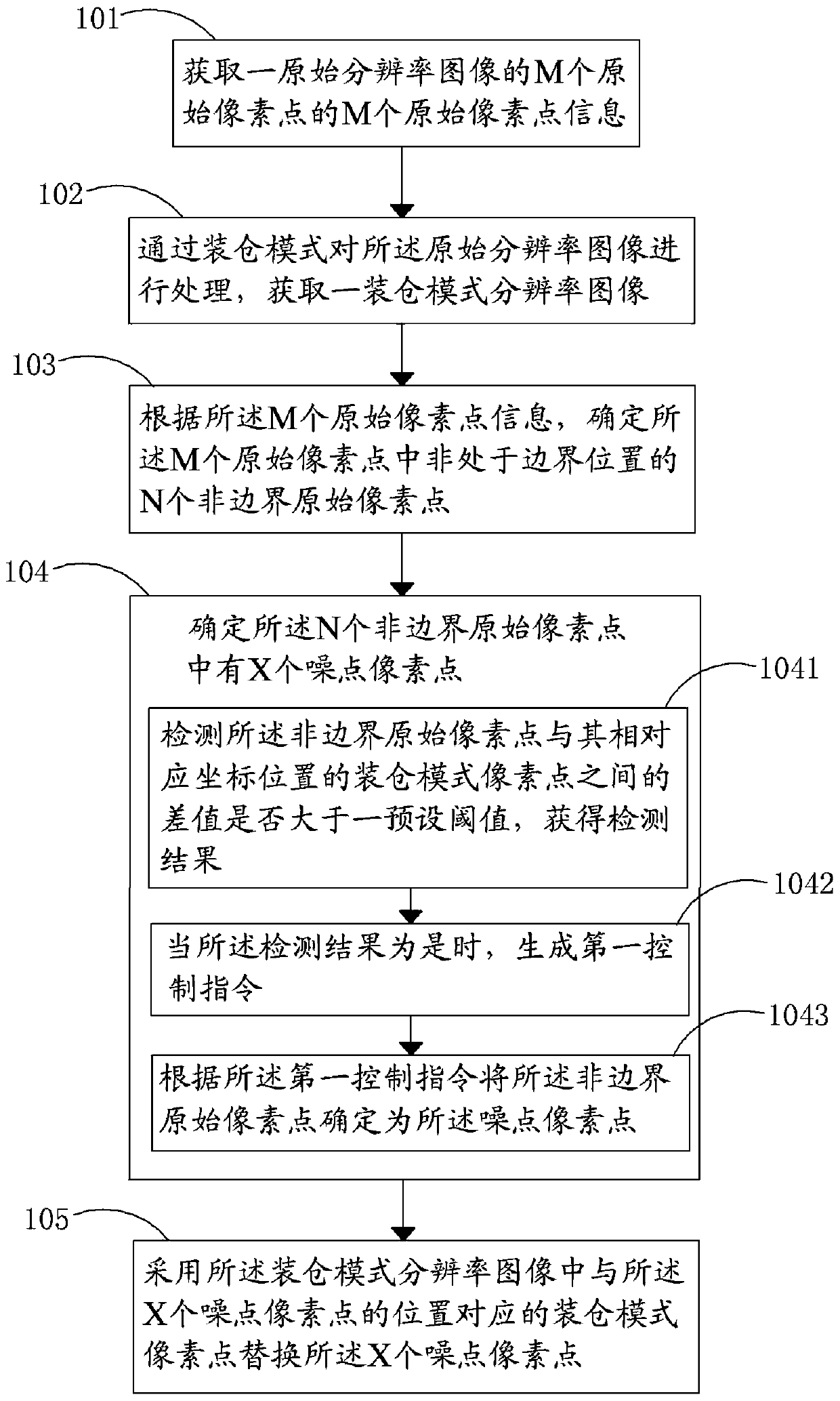
[0030] Please refer to figure 1 Embodiment 1 of the present application provides an information processing method, which is applied to an electronic device, and the method includes:

[0031]Step 101: Obtain M original pixel point information of M original pixel points of an original resolution image, where M is an integer greater than or equal to 1.

[0032] The original resolution image is for the specific hardware of the electronic device, for example, a camera with 300,000 pixels, the original resolution image acquired by the camera is an image with a resolution of 640*480, a For a 2-megapixel camera, the original resolution image acquired by the camera is a 1600*1200 resolution image.

[0033] It can be seen that the specific resolution of the original resolution image is determined by the hardware of the electronic device, and the technical solution of the present application does not limit the processing of specific resolution images, so the technical solution in the em...

Embodiment 2

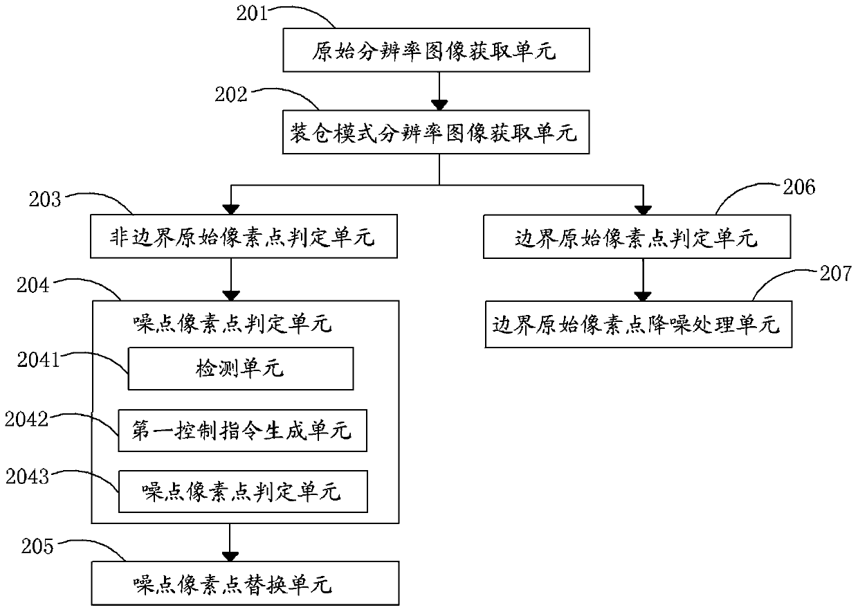
[0101] Please refer to figure 2 , Embodiment 2 of the present application provides an electronic device based on an information processing method, including:

[0102] The original resolution image acquisition unit is configured to acquire M original pixel point information of M original pixel points of an original resolution image, where M is an integer greater than or equal to 1.

[0103] The binning mode resolution image acquisition unit is used to process the original resolution image through the binning mode to obtain a binning mode resolution image, and the binning mode resolution image has M binning mode pixels , and the coordinate positions of the M binning pattern pixels are in one-to-one correspondence with the coordinate positions of the M original pixel points.


PUM


Abstract

The invention provides an information processing method and electronic equipment, and the method comprises the steps: obtaining the information of M original pixels of an original resolution image; carrying out the processing of the original resolution image in a mode of binning, and obtaining a binning-mode resolution image; determining N non-boundary original pixels which are not located at the boundary; determining X noise pixels in the N non-boundary original pixels; and replacing the X noise pixels through the binning-mode pixels corresponding to the positions of the X noise pixels. Because the method provided by the invention is short in processing flow of execution, is simple and easy in processing mode, is small in improvement of employed hardware and can achieve effective imaging without higher power consumption, the method solves technical problems that a multi-frame operation noise reduction method in the prior art is long in consumed time during photoelectric imaging and low in processing efficiency. The method is high in imaging efficiency, and is low in power consumption.

Description

technical field [0001] The invention relates to the field of electronic technology, in particular to an information processing method and electronic equipment. Background technique [0002] At present, in the field of electronic imaging technology, how to improve the photosensitive effect of the image sensor and suppress the formation of noise in the later image has always been the direction of the development of the optoelectronic imaging industry. [0003] For this reason, in the existing photoelectric imaging technology, various complex algorithms and high-cost hardware are usually used to suppress or reduce the noise in the image. For example, in CMOS mode, multi-frame calculation is used to reduce noise The method, this method realizes noise reduction by comparing multiple frames of imaging pictures, or uses CCD photosensitive element as imaging hardware, and adopts a unified output method to ensure the consistency of imaging signal output. [0004] However, during the...

Claims


Application Information

Patent Timeline
Patent Type & Authority Patents(China)
IPC IPC(8): H04N5/217H04N9/79
Inventor 于宙
Owner LENOVO (BEIJING) LTD
Learn More