Double-scanning-line pixel array structure, display panel, display device and drive method thereof
A pixel array and display panel technology, applied in nonlinear optics, instruments, optics, etc., can solve the problems of reducing pixel aperture ratio, inability to achieve single-point inversion, large resistance and capacitance load of data lines, etc., to improve display quality , Improve the aperture ratio and penetration rate, and reduce the effect of resistive and capacitive loads
- Summary
- Abstract
- Description
- Claims
- Application Information
AI Technical Summary
Problems solved by technology
Method used
Image

Examples
no. 1 example
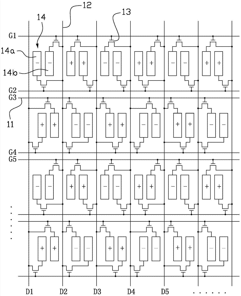
[0040] image 3 It is the equivalent circuit diagram of the double scan line pixel array structure in the first embodiment of the present invention, please refer to image 3 , the dual scan line pixel array structure includes a plurality of scan lines 21, a plurality of data lines and a plurality of sub-pixel electrodes 24, the plurality of scan lines 21 and the plurality of data lines are intersected, and the plurality of sub-pixel electrodes 24 are in an array distribution, that is, the plurality of sub-pixel electrodes 24 are distributed in multiple rows and columns.
[0041] Two scanning lines 21 are arranged between every two adjacent rows of sub-pixel electrodes 24 , and one scanning line 21 is respectively arranged above the first row of sub-pixel electrodes 24 and below the last row of sub-pixel electrodes 24 . Such as image 3 As shown, taking the two adjacent rows of sub-pixel electrodes 24 in the figure as an example, two scanning lines G2 and G3 are provided betw...
no. 2 example
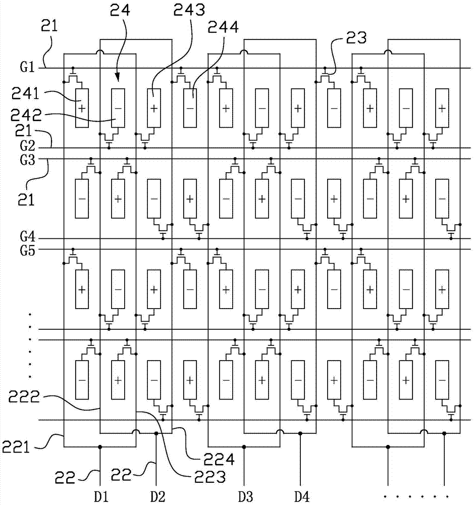
[0051] Figure 4 For the equivalent circuit diagram of the double scan line pixel array structure in the second embodiment of the present invention, please refer to Figure 4 , this embodiment differs from the first embodiment above in that:
[0052] Among the sub-pixel electrodes 24 located in odd rows, each sub-pixel electrode 24 is connected to the data line immediately on the right side of the sub-pixel electrode 24 . Such as Figure 4 As shown, taking all the sub-pixel electrodes 24 in the first row in the figure as an example, each sub-pixel electrode 24 is connected to the data line on the right side of the sub-pixel electrode 24, such as the first sub-pixel electrode 241 in the first row Connect to the data line 222 on the right side of the sub-pixel electrode 241, the second sub-pixel electrode 242 in the first row is connected to the data line 223 on the right side of the sub-pixel electrode 242, and the third sub-pixel in the first row The electrode 243 is connec...
PUM
 Abstract
Description
Claims
Application Information
 - Generate Ideas
- Intellectual Property
- Life Sciences
- Materials
- Tech Scout
- Unparalleled Data Quality
- Higher Quality Content
- 60% Fewer Hallucinations
Browse by: Latest US Patents, China's latest patents, Technical Efficacy Thesaurus, Application Domain, Technology Topic, Popular Technical Reports.
© 2025 PatSnap. All rights reserved.Legal|Privacy policy|Modern Slavery Act Transparency Statement|Sitemap|About US| Contact US: help@patsnap.com