
an optical module

An optical module and finger technology, which is applied in the field of optical communication, can solve the problems of length increase and achieve the effects of shortening length, reducing high-frequency attenuation, and ensuring receiving sensitivity

Active Publication Date: 2018-05-04
HISENSE BROADBAND MULTIMEDIA TECH
View PDF6 Cites 0 Cited by
  • Summary
  • Abstract
  • Description
  • Claims
  • Application Information

AI Technical Summary

Problems solved by technology

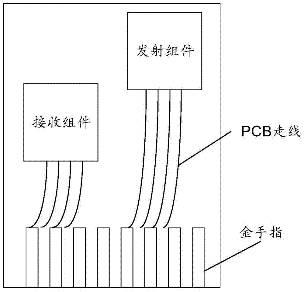
According to the radiation field energy spatial distribution theory, it can be known that the energy field is the strongest in its horizontal circle, so that the receiving component can effectively avoid the main energy radiated by the transmitting component, thereby reducing the interference of the transmitting component to the receiving component and improving the efficiency of the receiving component. The receiving sensitivity; however, this will increase the length of the connection between the transmitting component and the golden finger (ie, the PCB trace), and the longer the PCB trace, the more serious the high-frequency attenuation of the electrical signal on the PCB trace

Method used


Image

  • an optical module
  • an optical module
  • an optical module

Examples


Embodiment Construction

[0020] The technical solutions in the embodiments of the present invention will be described exemplarily below in conjunction with the accompanying drawings in the embodiments of the present invention. Obviously, the described embodiments are only some, not all, embodiments of the present invention. Based on the embodiments of the present invention, all other embodiments obtained by persons of ordinary skill in the art without making creative efforts belong to the protection scope of the present invention.

[0021] The "and / or" in the embodiment of the present invention is only an association relationship describing associated objects, indicating that there may be three relationships, for example, A and / or B, which may mean: A exists alone, and A and B exist at the same time , there are three cases of B alone. " / " generally means that the associated objects before and after are an "or" relationship. "Multilayer" means two or more layers; "plurality" means two or more layers. ...


PUM


Abstract

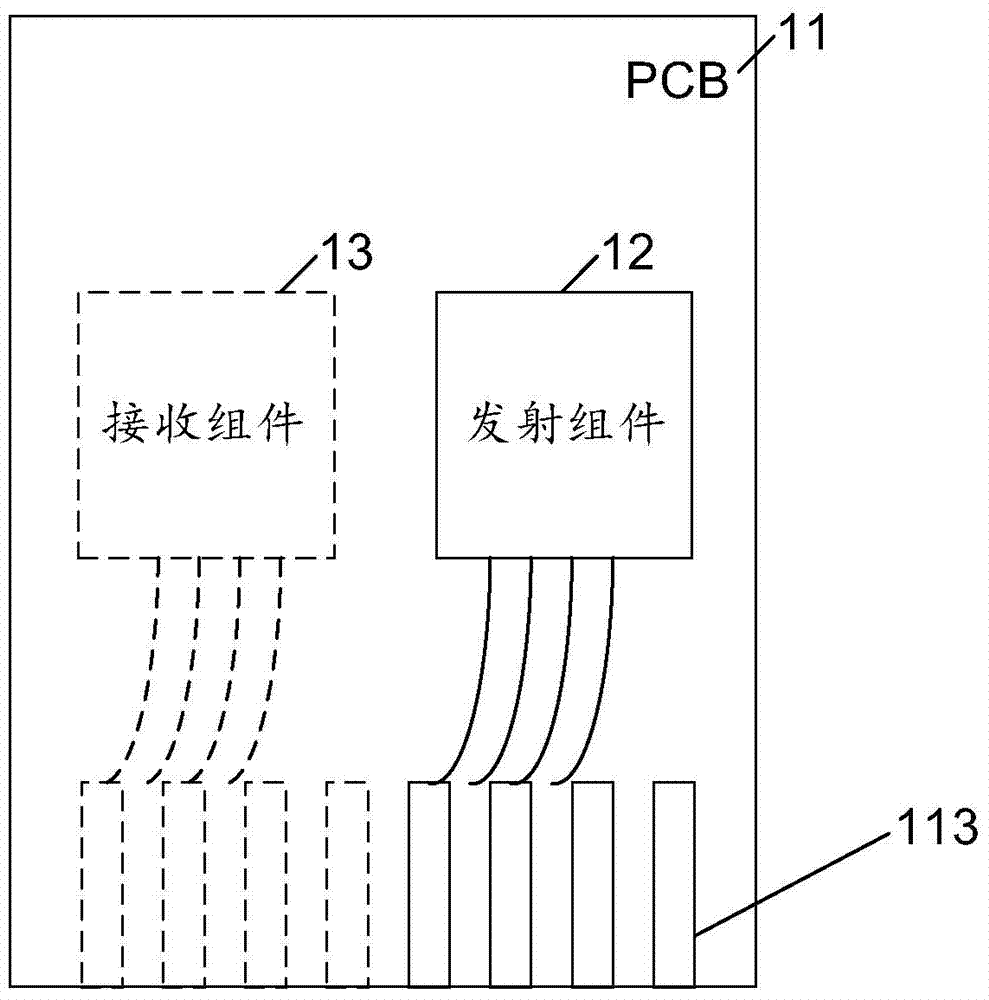
An optical module, which relates to the technical field of optical communications and is used for reducing the high frequency attenuation of an electrical signal on a PCB (11) wiring while guaranteeing the reception sensitivity. The optical module comprises: a PCB (11), wherein the PCB (11) comprises a first surface (111), a second surface (112) and a gold finger end (113) distributed with a plurality of gold fingers; a transmitting assembly (12) arranged on the first surface (111), wherein the transmitting assembly (12) is connected to the gold fingers; and a receiving assembly (13) arranged on the second surface (112), wherein the receiving assembly (13) is connected to the gold fingers. The PCB (11) further comprises a grounding layer. The optical module may be a receiving and transmitting integrated optical module.

Description

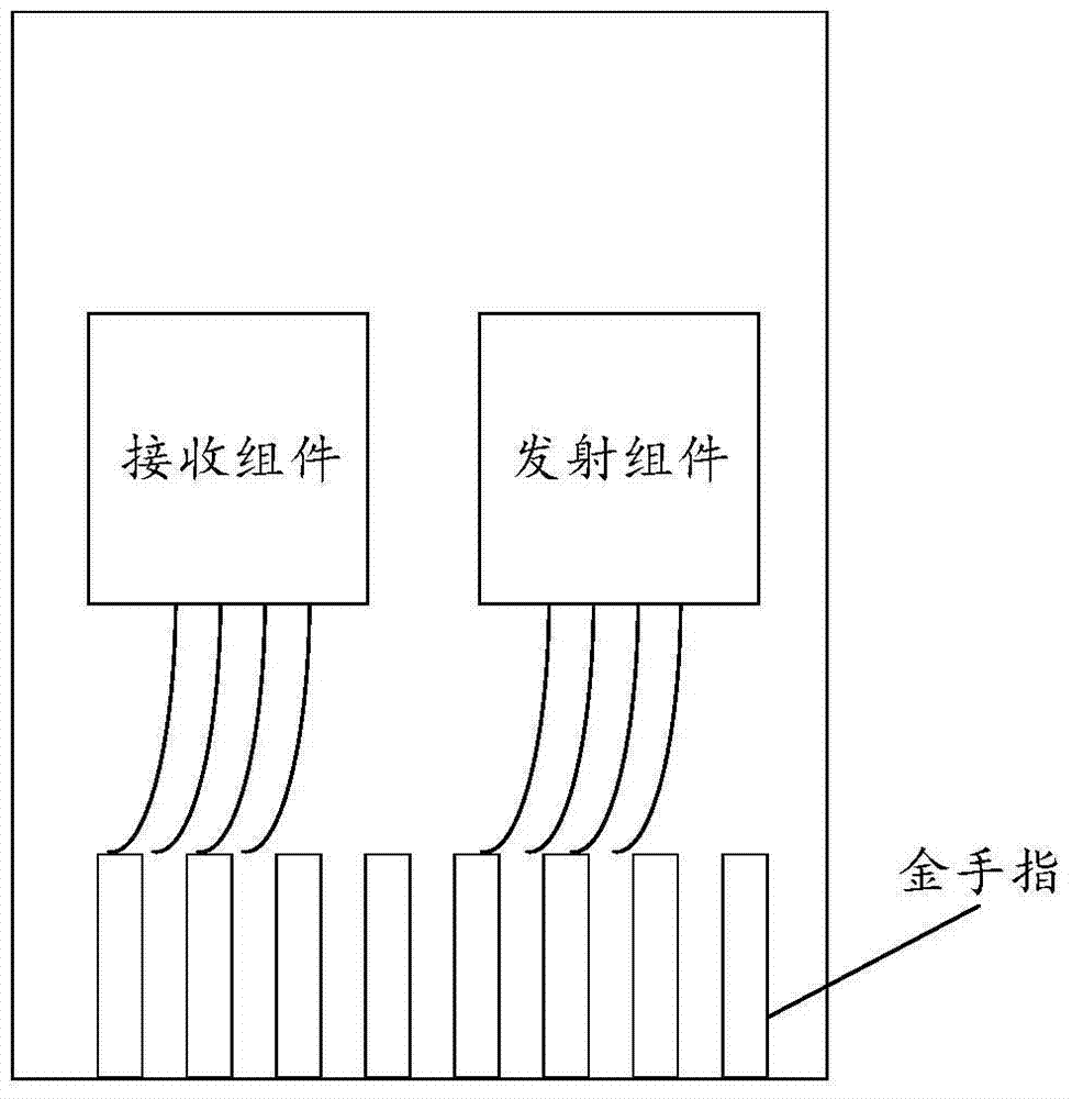
technical field [0001] The invention relates to the technical field of optical communication, in particular to an optical module. Background technique [0002] The optical module includes a transmitting component and a receiving component. At present, the transmitting component and the receiving component are generally arranged on the upper surface of a PCB (Printed Circuit Board, printed circuit board), such as figure 1 shown. In addition, multiple gold fingers are distributed on the gold finger end of the PCB, and both the transmitting component and the receiving component are connected to the gold fingers. The energy radiated from the wire (ie gold wire) between the driver chip and the laser in the transmitting component will cause interference to the receiving component, which will affect the receiving sensitivity of the receiving component. [0003] In order to solve the above problems, at present, the transmitting component and the receiving component are generally s...

Claims


Application Information

Patent Timeline
Patent Type & Authority Patents(China)
IPC IPC(8): G02B6/42
CPCG02B6/42
Inventor 贲仕建夏京盛杨思更
Owner HISENSE BROADBAND MULTIMEDIA TECH
Learn More