
Airtight parallel transmission optical device

An air-tight, light-transmitting technology, applied in the field of optical communication, can solve the problems of difficult to guarantee product reliability, difficult to achieve air-tight packaging, difficult to meet the requirements of packaging technology, etc., to achieve automatic production, increase density and capacity, Mount compact effect

Active Publication Date: 2016-03-16
WUHAN TELECOMM DEVICES
View PDF6 Cites 5 Cited by
  • Summary
  • Abstract
  • Description
  • Claims
  • Application Information

AI Technical Summary

Problems solved by technology

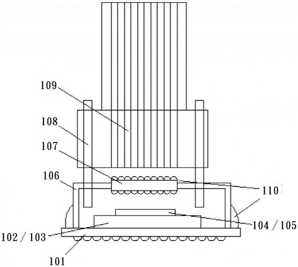
Two guide holes are usually designed on the cover for plugging and unplugging of the array fiber jumper 109 at the user end. The array fiber jumper 109 currently uses a standard guide pin 108, and the guide pin 108 is compatible with the guide on the cover. The holes are matched with high precision, and the entire device is packaged. The array chip can be 4-channel, 8-channel, 12-channel, or 24-channel products. In this design, the device is based on COB packaging technology, and the optical device is bound Fixed on the PCB board, since the entire product package is bonded with adhesive, it is difficult to achieve airtight packaging with this process based on the existing glue sealing process level, and in some places where the environment is relatively harsh, the reliability of the product is difficult to guarantee
In addition, if the channel density needs to be increased, the existing packaging technologies are difficult to meet the requirements

Method used


Image

  • Airtight parallel transmission optical device
  • Airtight parallel transmission optical device
  • Airtight parallel transmission optical device

Examples


Embodiment Construction

[0024] The present invention will be described in further detail below in conjunction with specific embodiments and accompanying drawings. Examples of the described embodiments are shown in the drawings, wherein like or similar reference numerals designate like or similar elements or elements having the same or similar functions throughout. The embodiments described below with reference to the accompanying drawings are exemplary, and are only used to explain the technical solution of the present invention, and should not be construed as limiting the present invention.

[0025] In the description of the present invention, the terms "inner", "outer", "longitudinal", "transverse", "upper", "lower", "top", "bottom" or "front", "rear", "left ", "right" and other indicated orientations or positional relationships are based on the orientations or positional relationships shown in the drawings, and are only for the convenience of describing the present invention and do not require tha...


PUM


Abstract

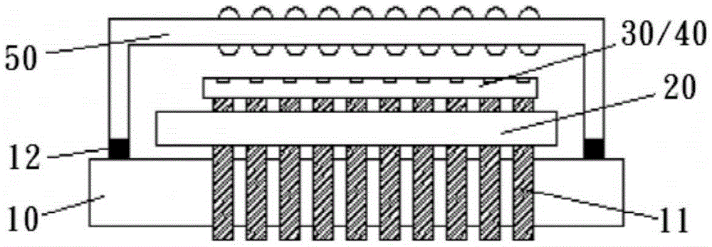
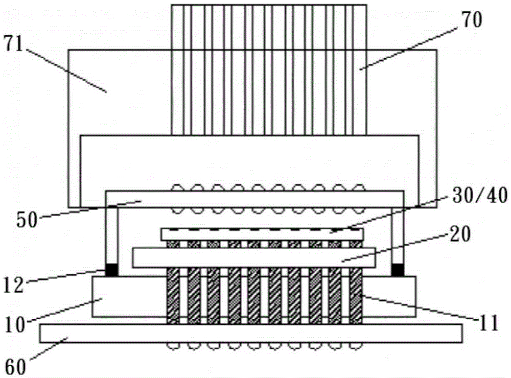
The invention provides an airtight parallel transmission optical device comprising a silicon substrate, an IC chip, a VCSEL chip, a PD chip, and a lens cover plate. The silicon substrate is provided with a silicon dioxide layer, and is provided with fine through holes, which are filled with conductive substances. The conductive substances are used to communicate the surface layer and the bottom layer of the silicon substrate, and are protruded from the bottom surface of the silicon substrate. The silicon substrate is also provided with a solder layer in a plated manner, and the IC chip is disposed on the silicon substrate in an inverted manner. The VCSEL chip and the PD chip are invertedly disposed on the IC chip in an attached manner. The lens cover plate is provided with an array lens, and is buckled with the silicon substrate by a high-precision image aligning system, and then is integrated with the solder layer by adopting the eutectic fusing technology, and then the lens array can be aligned with the VCSEL chip and the PD chip to realize the optical path coupling, and therefore the airtight packaging technology problem can be solved, the material-saving performance and the energy consumption-saving performance can be achieved, the production can be facilitated, and then the product quality can be improved.

Description

technical field [0001] The invention relates to the technical field of optical communication, and in particular provides an airtight parallel transmission optical device, which is applicable to the application of medium optical modules. Specifically, it involves high-density packaging design of devices, which can effectively improve the performance and reliability of optical devices. Background technique [0002] At present, with the rapid development of the optical communication field, many short-distance interconnection products are required to meet higher speed and higher capacity and adopt parallel transmission mode. In the existing technology, most of the products used in the industry have been packaged by COB, such as 1*1 single-channel products, 1*4 four-channel array products, 1*12 twelve-channel array products, etc. Such products are usually packaged in COB and realized through the adhesive process, but considering the high-density and large-capacity requirements o...

Claims


Application Information

Patent Timeline
Patent Type & Authority Applications(China)
IPC IPC(8): G02B6/42
CPCG02B6/4204G02B6/4237G02B6/4251G02B6/4266
Inventor 曹芳付永安
Owner WUHAN TELECOMM DEVICES
Learn More