Adjustable distributed amplifier circuit

A technology of distributed amplifiers and circuits, applied in the direction of improving amplifiers to reduce nonlinear distortion, amplification control, electrical components, etc., to achieve the effect of improving linearity and reducing the risk of processing verification failure

Active Publication Date: 2016-02-24
NANJING UNIV OF POSTS & TELECOMM
View PDF4 Cites 6 Cited by
  • Summary
  • Abstract
  • Description
  • Claims
  • Application Information

AI Technical Summary

Problems solved by technology

In traditional distributed amplifiers, each gain unit must work under the sam

Method used


Image

  • Adjustable distributed amplifier circuit
  • Adjustable distributed amplifier circuit
  • Adjustable distributed amplifier circuit

Examples


Embodiment Construction

[0026] In order to make the object, technical solution and advantages of the present invention clearer, the present invention will be further described in detail below in conjunction with the accompanying drawings and embodiments. It should be understood that the specific embodiments described here are only used to explain the present invention, not to limit the present invention.

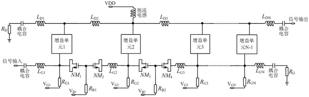
[0027] The present invention and figure 1 There are three improvements over the conventional distributed amplifier shown:

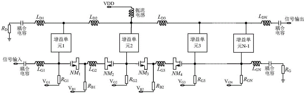
[0028] (1) In the input artificial transmission line, at least one group of adjacent two-stage gain units are connected in series with two NMOS transistors NM 2i-1 and NM 2i , with the on-chip inductance L G(i+1) Together form a band-pass matching network, the NMOS transistor NM 2i-1 and NM 2i The source and drain are connected together, through a large resistor R Bi connected to the bias voltage V Bi ,; figure 2 It is a structure of the distributed amplifier circuit ...


PUM


Abstract

The invention discloses an adjustable distributed amplifier circuit. The adjustable distributed amplifier circuit comprises a plurality of gain units, input on-chip inductors and output on-chip inductors, wherein the input on-chip inductors are connected to input ends of the gain units; the output on-chip inductors are connected to output ends of the gain units; two NMOS (N-Channel Metal Oxide Semiconductor) transistors are connected in series between the input ends of at least one group of two adjacent gain units; the NMOS transistors and the input on-chip inductors construct a band-pass matching network; respective source electrodes and drain electrodes of the two NMOS transistors are connected together; the NMOS transistors are connected to a bias voltage through a first bias resistor; and the input ends of the gain units are connected with second bias resistors in order to apply second bias voltages to the other ends of the second bias resistors. The NMOS transistors which can be equivalent to variable capacitors are introduced in order to isolate direct-current biases at the input ends of the gain units, so that the matching network input into an artificial transmission line can be debugged after processing. Thus, the risk of failure in processing verification due to factors such as poor modeling inaccuracy or process deviations is lowered.

Description

technical field [0001] The invention belongs to the technical field of integrated circuits, in particular to an adjustable distributed amplifier circuit. Background technique [0002] The rapid development of wireless communication technology puts forward higher requirements on the data transmission rate and bandwidth of the communication system. Commonly used broadband amplifier design techniques include negative feedback, balanced amplifiers, resistor matching, and active matching, etc., but none of these techniques can effectively improve the gain-bandwidth product of the amplifier. Due to its structural characteristics, the distributed amplifier can break through the limitation of the gain-bandwidth product of the amplifier and realize wider-band signal amplification. It is obtained in the field of ultra-wideband MMIC (Monolithic Microwave Integrated Circuit, monolithic microwave integrated circuit) a wide range of applications. Various types of structures have appeare...

Claims


Application Information

Patent Timeline
IPC IPC(8): H03F1/32H03G3/20
Inventor 张瑛
Owner NANJING UNIV OF POSTS & TELECOMM
Why Eureka
Try Eureka