A substrate for flexible optoelectronic devices and its preparation method
A technology of optoelectronic devices and substrates, which is applied in the fields of electrical solid devices, semiconductor/solid device manufacturing, electrical components, etc., and can solve the problem of poor bonding between flexible substrates and conductive layers, insufficient flexibility of flexible substrates, and poor water and oxygen barrier capabilities and other issues, to achieve the effect of improving light transmittance, improving water and oxygen barrier ability, and improving performance
- Summary
- Abstract
- Description
- Claims
- Application Information
AI Technical Summary
Problems solved by technology
Method used
Image

Examples
Embodiment 1
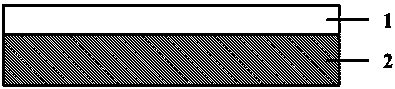
[0043] Such as figure 1 In the substrate structure shown, the flexible substrate 2 is a polyimide film doped with a mass ratio of 0.2% cationic UV-sensitive glue and 10% aloe vera gel, and the conductive layer 1 is graphene.
[0044] The preparation method is as follows:
[0045] ① First clean the rigid substrate with a surface roughness less than 1 nm, then use detergent, acetone, deionized water, and isopropanol to perform ultrasonic cleaning, and then dry it with dry nitrogen;
[0046] ② Prepare a mixed film of polyimide, cationic UV-sensitive glue and aloe gel by spin coating on a rigid substrate, with a film thickness of 5 μm. The raw material of the cationic UV-sensitive glue includes the following components:
[0047] Epoxy resin or modified epoxy resin 85 %
[0048] Thinner 10 %
[0049] Cationic photoinitiator 5 %;
[0050] ③ In ② surface spraying method, the graphene aqueous dispersion is prepared as a conductive layer, the height is 20 cm, the spraying pressure ...
Embodiment 2
[0056] Such as figure 1 In the substrate structure shown, the flexible substrate 2 is a polyimide film doped with a mass ratio of 0.5% cationic UV-sensitive glue and 15% aloe vera gel, and the conductive layer 1 is carbon nanotubes.
[0057] The preparation method is as follows:
[0058] ① First clean the rigid substrate with a surface roughness less than 1 nm, then use detergent, acetone, deionized water, and isopropanol to perform ultrasonic cleaning, and then dry it with dry nitrogen;
[0059] ② Prepare a mixed film of polyimide, cationic UV-sensitive glue and aloe gel by spin coating on a rigid substrate, with a film thickness of 20 μm. The cationic UV-sensitive glue raw material includes the following components:
[0060] Epoxy resin or modified epoxy resin 87 %
[0061] Thinner 9 %
[0062] Cationic photoinitiator 4 %;
[0063] ③ In ② surface spraying method, the carbon nanotube aqueous dispersion was prepared as a conductive layer, with a height of 20 cm, a spraying...
Embodiment 3
[0069] Such as figure 1 In the substrate structure shown, the flexible substrate 2 is a polystyrene film doped with a mass ratio of 2% cationic UV-sensitive glue and 23% aloe vera gel, and the conductive layer 1 is silver nanowires.
[0070] The preparation method is as follows:
[0071] ① First clean the rigid substrate with a surface roughness less than 1 nm, then use detergent, acetone, deionized water, and isopropanol to perform ultrasonic cleaning, and then dry it with dry nitrogen;
[0072] ② Prepare a mixed film of polystyrene, cationic UV-sensitive glue and aloe gel by spin coating on a rigid substrate, the film thickness is 60 μm, and the cationic UV-sensitive glue raw material includes the following components:
[0073] Epoxy resin or modified epoxy resin 89 %
[0074] Thinner 8 %
[0075] Cationic photoinitiator 3 %;
[0076] ③ On the surface of ②, the silver nanowire isopropanol dispersion was used to prepare a conductive layer with a height of 20 cm, a sprayin...
PUM
| Property | Measurement | Unit |
|---|---|---|
| thickness | aaaaa | aaaaa |
| surface roughness | aaaaa | aaaaa |
| thickness | aaaaa | aaaaa |
Abstract
Description
Claims
Application Information
 - Generate Ideas
- Intellectual Property
- Life Sciences
- Materials
- Tech Scout
- Unparalleled Data Quality
- Higher Quality Content
- 60% Fewer Hallucinations
Browse by: Latest US Patents, China's latest patents, Technical Efficacy Thesaurus, Application Domain, Technology Topic, Popular Technical Reports.
© 2025 PatSnap. All rights reserved.Legal|Privacy policy|Modern Slavery Act Transparency Statement|Sitemap|About US| Contact US: help@patsnap.com