Photoresistor and manufacturing method thereof
A technology of photosensitive resistors and manufacturing methods, which is applied in the direction of circuits, electrical components, semiconductor devices, etc., can solve the problems of reduced performance parameters of photosensitive resistors, high scrap rate, poor stability, etc., and achieve reduced scrap rate, small content, and high stability Effect
- Summary
- Abstract
- Description
- Claims
- Application Information
AI Technical Summary
Problems solved by technology
Method used
Image
Examples
Embodiment 1
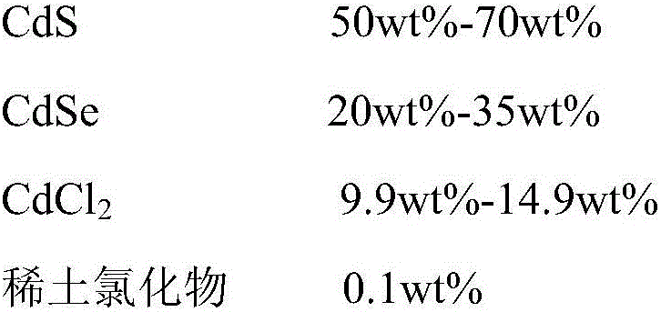
[0036] Embodiment 1: A photosensitive resistor, comprising a ceramic substrate, a photosensitive layer, and two electrodes. The photosensitive layer is coated on the surface of the ceramic substrate. The photosensitive layer and the ceramic substrate form the main body of the photosensitive resistor. The two electrodes are respectively mounted on two sides of the main body of the photosensitive resistor. At the end, the photosensitive layer is composed of the following components:
[0037]
[0038] The rare earth chloride is one of holmium chloride, neodymium chloride, gadolinium chloride, dysprosium chloride and samarium chloride, or a mixture of two or more.
Embodiment 2
[0039] Embodiment 2: A photosensitive resistor includes a ceramic substrate, a photosensitive layer and two electrodes. The photosensitive layer is coated on the surface of the ceramic substrate. The photosensitive layer and the ceramic substrate form the main body of the photosensitive resistor. The two electrodes are respectively mounted on the two sides of the main body of the photosensitive resistor. At the end, the photosensitive layer is composed of the following components:
[0040]
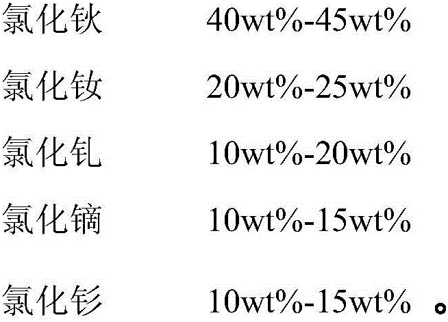
[0041] In this embodiment, the rare earth chloride is a mixture of holmium chloride, neodymium chloride, gadolinium chloride, dysprosium chloride and samarium chloride, and the rare earth chloride is composed of the following components:
[0042]
[0043] In this embodiment, the thickness of the photosensitive layer is 5 microns.
[0044] In this embodiment, the ceramic substrate is made of aluminum oxide with a purity of more than 93%.
Embodiment 3
[0045] Embodiment 3: A photosensitive resistor, comprising a ceramic substrate, a photosensitive layer and two electrodes. The photosensitive layer is coated on the surface of the ceramic substrate. The photosensitive layer and the ceramic substrate form the main body of the photosensitive resistor. The two electrodes are respectively mounted on two sides of the main body of the photosensitive resistor. At the end, the photosensitive layer is composed of the following components:
[0046]
[0047]
[0048] In this embodiment, the rare earth chloride is a mixture of holmium chloride, neodymium chloride, gadolinium chloride, dysprosium chloride and samarium chloride, and the rare earth chloride is composed of the following components:
[0049]
[0050] In this embodiment, the thickness of the photosensitive layer is 2 microns.
[0051] In this embodiment, the ceramic substrate is made of aluminum oxide with a purity of more than 93%.
PUM
 Abstract
Description
Claims
Application Information
 - R&D Engineer
- R&D Manager
- IP Professional
- Industry Leading Data Capabilities
- Powerful AI technology
- Patent DNA Extraction
Browse by: Latest US Patents, China's latest patents, Technical Efficacy Thesaurus, Application Domain, Technology Topic, Popular Technical Reports.
© 2024 PatSnap. All rights reserved.Legal|Privacy policy|Modern Slavery Act Transparency Statement|Sitemap|About US| Contact US: help@patsnap.com


