
Rapid annealing method of power device and the power device

A power device, rapid annealing technology, applied in semiconductor/solid-state device manufacturing, electrical components, circuits, etc., can solve the problems of limiting the performance of power devices, high cost of use, increasing device manufacturing costs, etc., to improve process flexibility, reduce Manufacturing cost, effect of increasing activation rate

Inactive Publication Date: 2016-02-17
PEKING UNIV FOUNDER GRP CO LTD +1
View PDF7 Cites 0 Cited by
  • Summary
  • Abstract
  • Description
  • Claims
  • Application Information

AI Technical Summary

Problems solved by technology

[0009] Although the laser rapid thermal annealing treatment is very effective for the activation of implanted ions on the back of the power device, the laser annealing equipment is expensive and the cost of use is higher than that of ordinary rapid annealing equipment, which increases the manufacturing cost of the device.
At the same time, in order to reduce the impact on the front metal, the time and temperature of laser rapid thermal annealing will still be limited, which also affects the process flexibility and limits the further improvement of power device performance.

Method used


Image

  • Rapid annealing method of power device and the power device

Examples


Embodiment Construction

[0016] In order to understand the above-mentioned purpose, features and advantages of the present invention more clearly, the present invention will be further described in detail below in conjunction with the accompanying drawings and specific embodiments. It should be noted that, in the case of no conflict, the embodiments of the present application and the features in the embodiments can be combined with each other.

[0017] In the following description, many specific details are set forth in order to fully understand the present invention, but the present invention can also be implemented in other ways different from those described here, therefore, the present invention is not limited to the specific embodiments disclosed below limit.

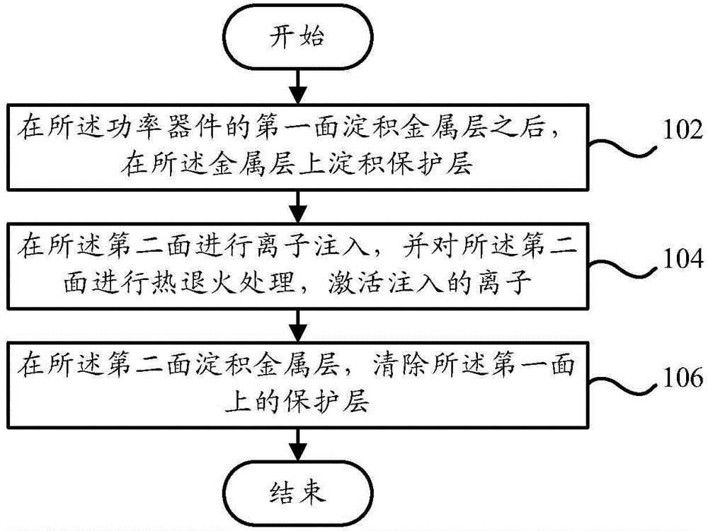
[0018] figure 1 A schematic flowchart of a rapid annealing method for a power device according to an embodiment of the present invention is shown.

[0019] like figure 1 As shown, the rapid annealing method for a power device according ...


PUM

PropertyMeasurementUnit
thicknessaaaaaaaaaa

Abstract

The invention provides a rapid annealing method of a power device and one power device. The rapid annealing method of the power device comprises the following steps of depositing a metal layer on a first surface of the power device and then depositing a protective layer on the metal layer; carrying out ion implantation on a second surface, carrying out heat annealing processing on the second surface and activating implanted ions; depositing the metal layer on the second surface and removing the protective layer on the first surface. By using a technical scheme of the invention, after a making technology on the first surface of the power device is completed, the protective layer is deposited on the first surface of the power device so that protection to the making technology on the first surface of the power device during an annealing process is realized; power device performance is increased; simultaneously, conventional annealing processing is used and making cost is reduced.

Description

technical field [0001] The invention relates to the technical field of semiconductor devices and their manufacturing techniques, in particular to a rapid annealing method for a power device and a power device. Background technique [0002] In the process of making power devices, after completing the front-side process of the silicon wafer, in order to form the emitter on the back of the power device and reduce the contact resistance, it is often necessary to thin the back of the silicon wafer and then perform ion implantation, but in ion implantation Finally, a rapid thermal annealing must be performed on the silicon wafer. This rapid thermal annealing process can repair the damage caused by the implanted ions to the power device and activate the implanted ions at the same time. However, if the thermal annealing treatment is carried out by the traditional rapid thermal annealing method, the metal layer formed on the front side of the silicon wafer will melt when the power de...

Claims


Application Information

Patent Timeline
Patent Type & Authority Applications(China)
IPC IPC(8): H01L21/02H01L21/265
Inventor 李理马万里赵圣哲
Owner PEKING UNIV FOUNDER GRP CO LTD
Learn More