Piece type OGS touch screen and manufacturing method therefor
A technology of touch screen and manufacturing process, applied in the field of capacitive touch screen, which can solve the problems of low strength of OGS touch screen glass, cumbersome manufacturing process, and difficult shape processing, etc., and achieve the effects of environmental protection, optimization of manufacturing process, and improvement of glass strength
- Summary
- Abstract
- Description
- Claims
- Application Information
AI Technical Summary
Problems solved by technology
Method used
Image
Examples
Embodiment 1
[0050] This embodiment is used to illustrate the OGS touch screen of the present invention and its manufacturing method.
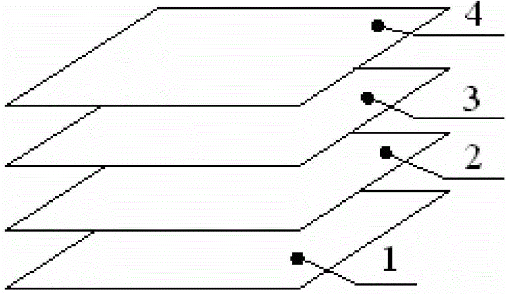
[0051] The manufacturing method of the OGS touch screen of the chip manufacturing process of the present embodiment comprises the following steps:
[0052] (1) Form the ink layer 2 on the transparent substrate 1: divide the transparent substrate 1 (that is, a small piece of chemically strengthened glass substrate) into a window area and a non-window area, and use a 400-mesh screen to print an ink layer on the non-window area of the transparent substrate 1 The laser-resistant black ink with a layer thickness of 4 μm is baked after printing. The baking temperature is 160 ° C and the baking time is 12 minutes. After the first layer of black ink layer is formed, a layer of laser-resistant ink with a thickness of 4 μm is printed. The black ink is baked after printing. The baking temperature is 160°C and the baking time is 12 minutes to form a bottom ink layer...
Embodiment 2
[0058] This embodiment is used to illustrate the OGS touch screen of the present invention and its manufacturing method.
[0059] The manufacturing method of the OGS touch screen of the chip manufacturing process of the present embodiment comprises the following steps:
[0060] (1) Form the ink layer 2 on the transparent substrate 1: Divide the transparent substrate 1 (that is, a small piece of chemically strengthened glass substrate) into a window area and a non-window area, and use a 350-mesh screen to print on the non-window area of the transparent substrate 1 first. High-temperature-resistant white ink with a layer thickness of 6 μm is baked after printing. The baking temperature is 150 ° C and the baking time is 15 minutes. After the first white ink layer is formed, a layer of high-temperature resistant white ink with a thickness of 6 μm is printed. The white ink is baked after printing. The baking temperature is 150°C and the baking time is 15 minutes. After the second...
Embodiment 3
[0066] This embodiment is used to illustrate the OGS touch screen of the present invention and its manufacturing method.
[0067] The manufacturing method of the OGS touch screen of the chip manufacturing process of the present embodiment comprises the following steps:
[0068] (1) Form the ink layer 2 on the transparent substrate 1: Divide the transparent substrate 1 (that is, a small piece of chemically strengthened glass substrate) into a window area and a non-window area, and use a 420-mesh screen to print an ink layer on the non-window area of the transparent substrate 1 High-temperature-resistant red ink with a layer thickness of 5 μm is baked after printing. The baking temperature is 180 ° C and the baking time is 10 minutes. After the first layer of red ink layer is formed, it is printed and baked in the same way. Form four layers of high-temperature-resistant red ink layers with a thickness of 5 μm in sequence, and then print a layer of laser-resistant gray ink with...
PUM
 Abstract
Description
Claims
Application Information
 - R&D
- Intellectual Property
- Life Sciences
- Materials
- Tech Scout
- Unparalleled Data Quality
- Higher Quality Content
- 60% Fewer Hallucinations
Browse by: Latest US Patents, China's latest patents, Technical Efficacy Thesaurus, Application Domain, Technology Topic, Popular Technical Reports.
© 2025 PatSnap. All rights reserved.Legal|Privacy policy|Modern Slavery Act Transparency Statement|Sitemap|About US| Contact US: help@patsnap.com

