
MEMS device for preventing suspension layer etching damage

A technology for suspended layers and devices, applied in the direction of electric solid devices, semiconductor devices, piezoelectric devices/electrostrictive devices, etc., can solve problems such as damage to the bottom of the movable structure layer, avoid etching backsplash damage, and ensure integrity The effect of sex, the realization method is simple

Active Publication Date: 2016-02-03
EAST CHINA INST OF OPTOELECTRONICS INTEGRATEDDEVICE
View PDF11 Cites 21 Cited by
  • Summary
  • Abstract
  • Description
  • Claims
  • Application Information

AI Technical Summary

Problems solved by technology

[0004] The purpose of the present invention is to overcome the existing MEMS device in the etching process, the etching ions accumulate on the surface of silicon dioxide, generate a reverse electric field, cause the direction of the etching ions to change, and cause a large impact on the bottom of the movable structure layer. The defect of damage, proposes a kind of MEMS device that prevents suspension layer etching damage, another object of the present invention provides a kind of MEMS device fabrication method that prevents suspension layer etching damage exactly

Method used


Image

  • MEMS device for preventing suspension layer etching damage
  • MEMS device for preventing suspension layer etching damage
  • MEMS device for preventing suspension layer etching damage

Examples


Embodiment Construction

[0024] The present invention will be further described below in conjunction with the accompanying drawings.

[0025] Such as Figure 13 As shown, a MEMS device for preventing etching damage of the suspension layer provided by the present invention is composed of an SOI silicon wafer substrate, a movable structure layer 8 and a cap silicon wafer 10,

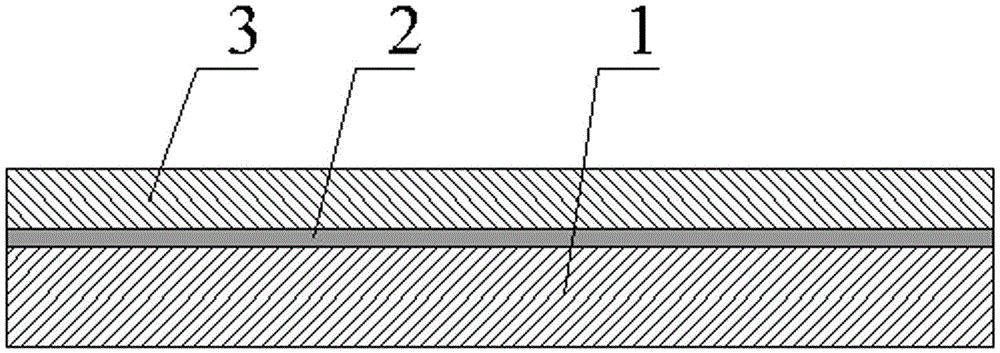
[0026] The substrate is made of SOI silicon wafer (composed of substrate silicon 1, buried oxide layer 2 and top layer silicon 3), and the top layer silicon 3 of the SOI silicon wafer is made of N-type or P-type low-resistance silicon with a resistivity of 0.001Ω cm-0.5Ω cm;

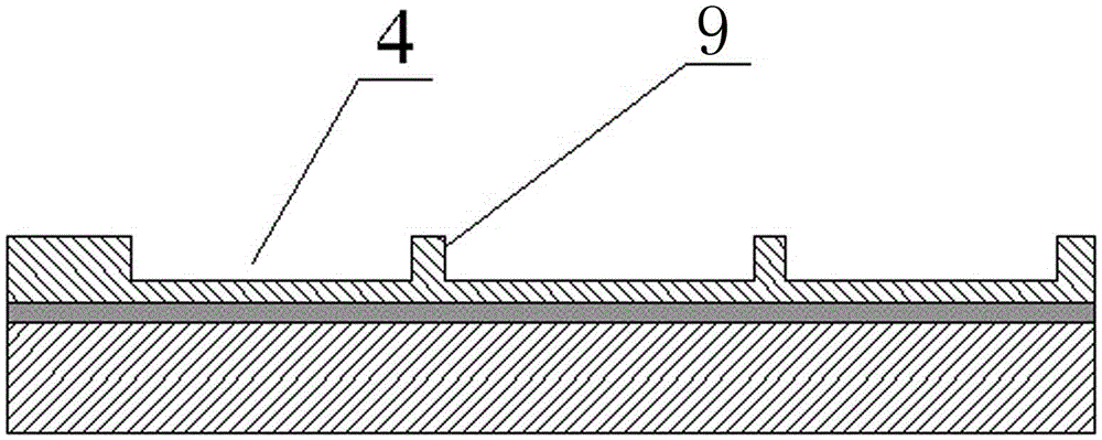
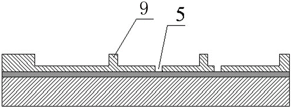
[0027] A shallow cavity 4, an electrode 9 (also called a lower electrode) and an electrode isolation groove 5 are provided on the surface of the top layer silicon 3 of the SOI silicon wafer of the substrate, and a first oxide layer 6 and a second oxide layer 7 are provided on the surface of the shallow cavity 4. The thickness of the first oxide layer 6 is ...


PUM

PropertyMeasurementUnit
Resistivityaaaaaaaaaa

Abstract

The invention relates to an MEMS device for preventing suspension layer etching damage, wherein a shallow cavity (4), an electrode (9) and an electrode isolation groove (5) are arranged on the surface of substrate silicon (3), a first oxide layer (6) with a thickness of 1500-5000 angstroms and a second oxide layer (7) with a thickness of 500-1500 angstroms are arranged on the surface of the shallow cavity (4), and a movable structural layer (8) is bonded on SOI silicon wafer top layer silicon (3) of the substrate; and a cap silicon wafer (10) is bonded with the SOI silicon wafer top layer silicon (3) of the substrate through glass frit (11) to achieve wafer level vacuum package. Compared with traditional MEMS devices, the MEMS device provided by the invention has the advantages that, a stepped silicon dioxide layer is used for protecting a lower electrode structure to not only well protect the lower electrode structure from being etched, but also avoid etching back splash damage of the structural layer and guarantee the integrity of the movable structure, the implementation method of the device structure is simple and feasible, and a standard process is convenient to form.

Description

technical field [0001] The invention belongs to the technical field of micro-electronic machinery, and in particular relates to a MEMS structure for preventing etching damage of a suspension structure. Background technique [0002] Micro-Electro-Mechanical Systems (MEMS) is an interdisciplinary technology developed on the basis of microelectronics technology. It uses photolithography, etching, film formation, bonding and other micro-processing methods to form electro-mechanical structures. , materials, machinery, physics, chemistry, biology and other fields. MEMS has attracted widespread attention due to its many advantages such as miniaturization, low power consumption, and mass production, and has been widely cited in the fields of automotive electronics, smart terminals, Internet of Things, and biomedicine. [0003] Compared with semiconductor integrated circuits, MEMS devices generally include movable mechanical structures. At present, the MEMS manufacturing process is ...

Claims


Application Information

Patent Timeline
IPC IPC(8): B81B3/00B81B7/00B81C1/00B81C3/00
Inventor 何凯旋郭群英黄斌宋东方段宝明陈璞王鹏刘磊
Owner EAST CHINA INST OF OPTOELECTRONICS INTEGRATEDDEVICE
Learn More