A method for preventing burrs and warping of gold fingers on pcb
A gold-finger lead and gold-finger technology, which is applied to the formation of electrical connection of printed components, electrical connection of printed components, printed circuit components, etc., can solve the problems of burrs or warping of gold finger leads, so as to improve warping and ensure quality , Improve the effect of burrs
- Summary
- Abstract
- Description
- Claims
- Application Information
AI Technical Summary
Problems solved by technology
Method used
Image
Examples
Embodiment
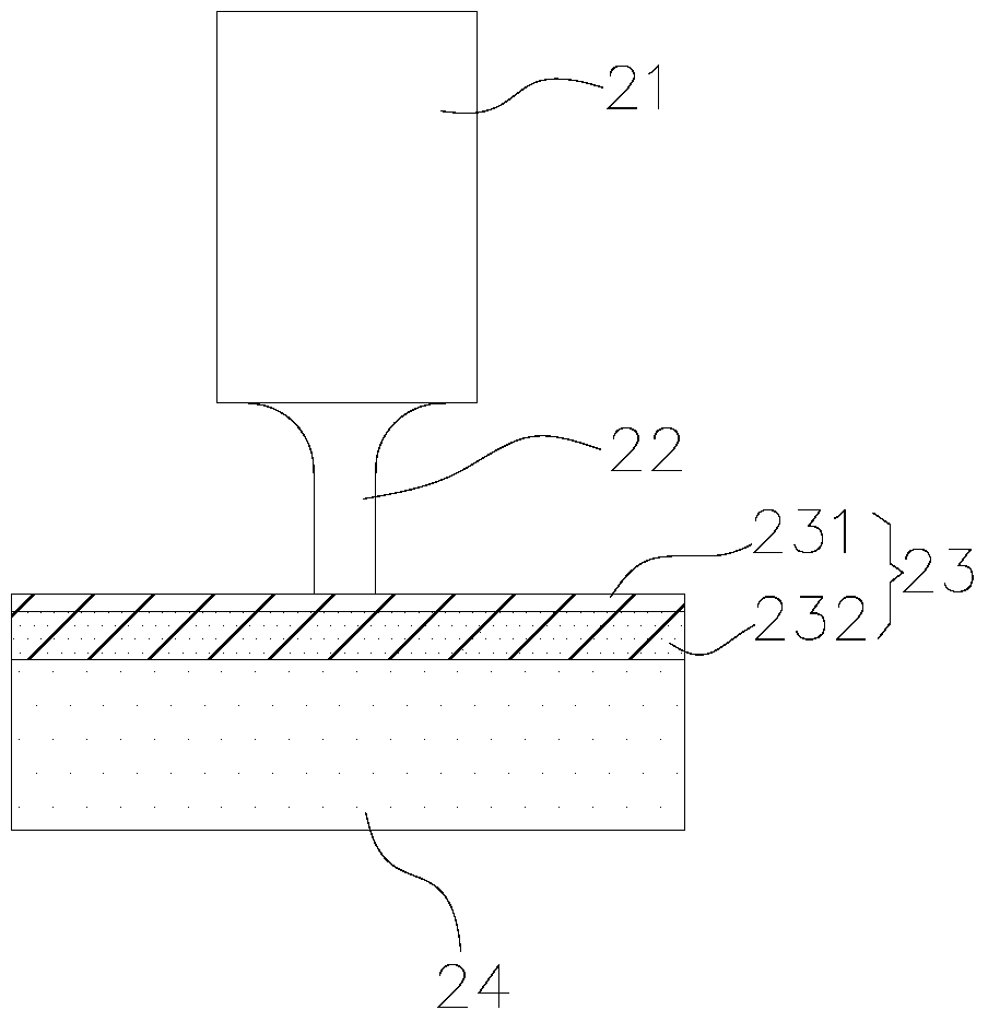
[0018] refer to image 3 , the present embodiment provides a method for preventing burrs and warping of the golden fingers on the PCB. 23 and gong empty area 24.
[0019] The PCB uses the positive film process to make the outer layer circuit. In the graphics drawn on the film, the width of the gold finger guide graphic is designed to be 0.25±0.025mm, and the end connecting the gold finger guide graphic and the gold finger graphic is designed as a horn shape. That is to say, both sides of the golden finger guide line figure are arc-shaped, and the radius of the circle where the arc is located is 0.3mm, and the central angle corresponding to the arc of the present embodiment is 90° (in other implementations, the corresponding arc can also be designed The central angle n of the film is 0<n≤90°); the hypotenuse area graphics and the gong empty area graphics are drawn on the film according to conventional techniques; through the exposure and development process, the graphics on th...
PUM
 Abstract
Description
Claims
Application Information
 - R&D
- Intellectual Property
- Life Sciences
- Materials
- Tech Scout
- Unparalleled Data Quality
- Higher Quality Content
- 60% Fewer Hallucinations
Browse by: Latest US Patents, China's latest patents, Technical Efficacy Thesaurus, Application Domain, Technology Topic, Popular Technical Reports.
© 2025 PatSnap. All rights reserved.Legal|Privacy policy|Modern Slavery Act Transparency Statement|Sitemap|About US| Contact US: help@patsnap.com


