
Large-diameter plane optical element defect three-dimensional fast dark field detection device and method

A technology for optical components and dark field detection, applied in the direction of optical testing flaws/defects, etc., can solve the problem of not being able to detect the depth information of defects, and achieve the effect of improving detection efficiency and easy implementation.

Active Publication Date: 2015-12-16
SHANGHAI INST OF OPTICS & FINE MECHANICS CHINESE ACAD OF SCI
View PDF7 Cites 23 Cited by
  • Summary
  • Abstract
  • Description
  • Claims
  • Application Information

AI Technical Summary

Problems solved by technology

[0003] The purpose of the present invention is to improve the problem that the defect depth information cannot be detected in the existing optical component detection technology, and to provide a three-dimensional fast dark field detection device and method for large-diameter planar optical component defects

Method used


Image

  • Large-diameter plane optical element defect three-dimensional fast dark field detection device and method
  • Large-diameter plane optical element defect three-dimensional fast dark field detection device and method
  • Large-diameter plane optical element defect three-dimensional fast dark field detection device and method

Examples


Embodiment Construction

[0017] The present invention will be described in detail below in conjunction with the accompanying drawings and embodiments, but the protection scope of the present invention should not be limited thereby.

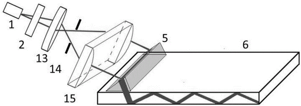
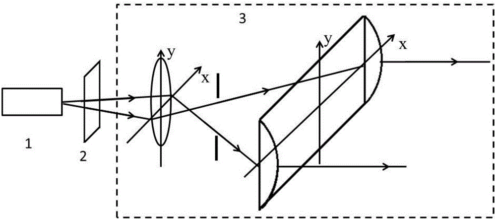
[0018] Such as figure 1 As shown, the three-dimensional rapid dark-field detection device for large-diameter planar optical elements of the present invention includes an illumination light source, a polarizer, a collimator lens system, a one-dimensional electronically controlled light source adjustment bracket, a right-angle prism, and a large-diameter planar optical element to be tested. 1. One-dimensional electronically controlled translation One-dimensional electronically controlled translational object platform, analyzer, imaging lens, CCD, computer, box. Among them, the lighting source, polarizer, and collimating lens system are arranged in sequence and installed on the one-dimensional electric light source adjustment bracket; On the electronically controlled transl...


PUM


Abstract

The invention provides a large-diameter plane optical element defect three-dimensional fast dark field detection device and method. The detection device comprises an illuminating light source, a polarizer, a collimating lens system, a one-dimensional electronic control light source adjusting support supporting system, a prism, a to-be-detected large-diameter plane optical element, a one-dimensional electronic control horizontal movement object support, a polarization analyzer, an imaging lens, a CCD, a computer and a box. Coordinate transformation is achieved through the Snell law, defect (or damage) position detection in the z axis direction can be achieved, and the problem that in the prior art, deep detection of the defect (or damage) in the optical element cannot be performed; detection speed is greatly increased, the device and method can be more effective for the large-diameter optical element, and the problem that in the prior art, time consumed during detection of the large-diameter optical element is long is effectively solved.

Description

technical field [0001] The invention relates to optical element defect detection, in particular to a three-dimensional fast dark field detection device and method for large-diameter planar optical element defects. Background technique [0002] Large-aperture optical components are one of the main components of high-power laser driver systems, and their surface defects (or damage) and scratches will directly affect the energy load capacity of the laser system. Focus on and analyze objects during the process. At present, component suppliers at home and abroad still mainly use the visual method to manually inspect components. Laboratories that develop high-power laser devices at home and abroad, including the Lawrence Livermore National Laboratory (LLNL) in the United States, are also developing two-dimensional imaging of surface defects (or damage) and scratches on large-aperture optical components. system. Existing research is limited to the detection of component surface ...

Claims


Application Information

Patent Timeline
Patent Type & Authority Applications(China)
IPC IPC(8): G01N21/88
Inventor 缪洁陈东贤谢雨江张雪洁崔子健杨朋千刘德安朱健强
Owner SHANGHAI INST OF OPTICS & FINE MECHANICS CHINESE ACAD OF SCI
Learn More