
How to make a mems device

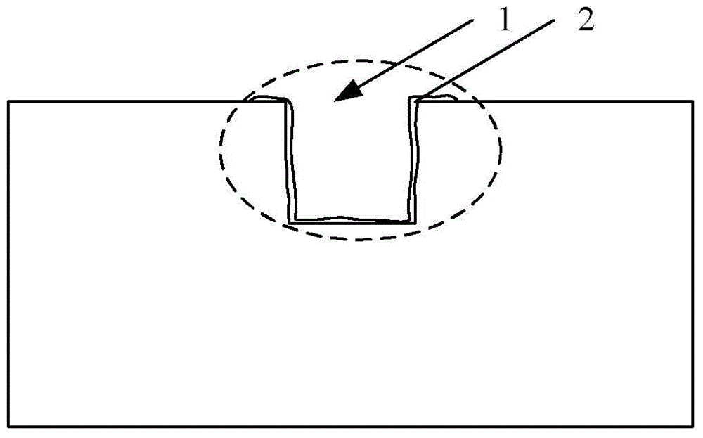
A manufacturing method and device technology, applied in the manufacture of microstructure devices, techniques for producing decorative surface effects, decorative art, etc., can solve the problem of the critical size of the opening 1, the side wall of the opening 1 is not ideal, and the yield rate is difficult to obtain, etc. problems, to avoid surface roughness, smooth side walls, and improve yield

Active Publication Date: 2017-03-01
SHANGHAI HUAHONG GRACE SEMICON MFG CORP
View PDF8 Cites 0 Cited by
  • Summary
  • Abstract
  • Description
  • Claims
  • Application Information

AI Technical Summary

Problems solved by technology

Depend on figure 1 It can be seen that the side wall of opening 1 is not ideal and is relatively rough, which also affects the critical dimension of opening 1
Therefore, it is difficult to obtain a better yield rate for the MEMS device structure made by the existing technology

Method used

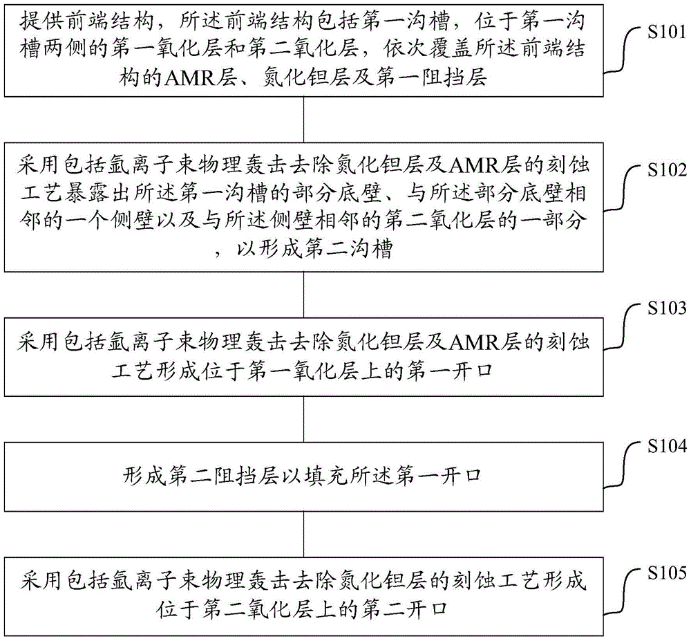
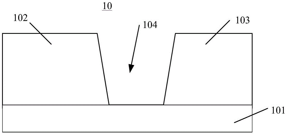

Image

  • How to make a mems device
  • How to make a mems device
  • How to make a mems device

Examples


Embodiment Construction

[0041] The manufacturing method of MEMS device of the present invention will be described in more detail below in conjunction with schematic diagram, wherein represents preferred embodiment of the present invention, should be appreciated that those skilled in the art can revise the present invention described here, and still realize the advantage of the present invention Effect. Therefore, the following description should be understood as the broad knowledge of those skilled in the art, but not as a limitation of the present invention.

[0042] In the following paragraphs the invention is described more specifically by way of example with reference to the accompanying drawings. Advantages and features of the present invention will be apparent from the following description and claims. It should be noted that all the drawings are in a very simplified form and use imprecise scales, and are only used to facilitate and clearly assist the purpose of illustrating the embodiments of...


PUM


Abstract

The invention discloses a manufacturing method for an MEMS (Micro-Electrico-Mechanical-System) device. The method comprises the following step: in a manufacturing process of the MEMS device, removing a partially-exposed tantalum nitride layer and an AMR (Anisotropic Magnet Resistive) layer below by adopting argon ion beam physical bombardment. The problem that polymers are generated easily due to etching of the tantalum nitride layer in the prior art is solved, so that the side wall of an opening formed by etching is flat; the opening is accurate; and the yield of a product is increased.

Description

technical field [0001] The invention relates to the technical field of semiconductors, in particular to a manufacturing method of a MEMS device. Background technique [0002] In recent years, with the development of micro-electromechanical system (Micro-Electrico-Mechanical-System, MEMS) technology, various micro-electromechanical devices, including: micro-sensors, micro-actuators, etc., have achieved miniaturization, which is beneficial to Improve device integration, so MEMS has become one of the main development directions. [0003] Nowadays, microelectromechanical systems manufactured using anisotropic magnet resistive (AMR) have the characteristics of high sensitivity, good thermal stability, low material cost, and simple preparation process, and have been widely used. [0004] The manufacturing process of the MEMS device in the prior art involves forming an AMR material layer, a tantalum nitride layer and a barrier layer on the front-end structure, wherein the barrier ...

Claims


Application Information

Patent Timeline
Patent Type & Authority Patents(China)
IPC IPC(8): B81C1/00
Inventor 张振兴
Owner SHANGHAI HUAHONG GRACE SEMICON MFG CORP
Learn More