Inner Layer Monitoring Structure of Multilayer Printed Circuit Board

A multi-layer printing and circuit board technology, applied in the directions of printed circuit components, other printed circuit components, circuit inspection/identification, etc. Reflect and other problems to achieve the effect of accurate alignment

Active Publication Date: 2018-07-06
竞陆电子(昆山)有限公司
View PDF7 Cites 0 Cited by
  • Summary
  • Abstract
  • Description
  • Claims
  • Application Information

AI Technical Summary

Problems solved by technology

[0003] However, although the current slicing hole can reflect some data of the inner layer, it cannot reflect the alignment between layers, that is, the defect of interlayer offset cannot be reflected at the slicing hole.
Currently, perspective machines are mostly used to detect interlayer offsets, and position scanning is performed on the positioning points on the work sheet to determine the offset. However, this detection method is slightly more expensive.

Method used


Image

  • Inner Layer Monitoring Structure of Multilayer Printed Circuit Board
  • Inner Layer Monitoring Structure of Multilayer Printed Circuit Board
  • Inner Layer Monitoring Structure of Multilayer Printed Circuit Board

Examples


Embodiment

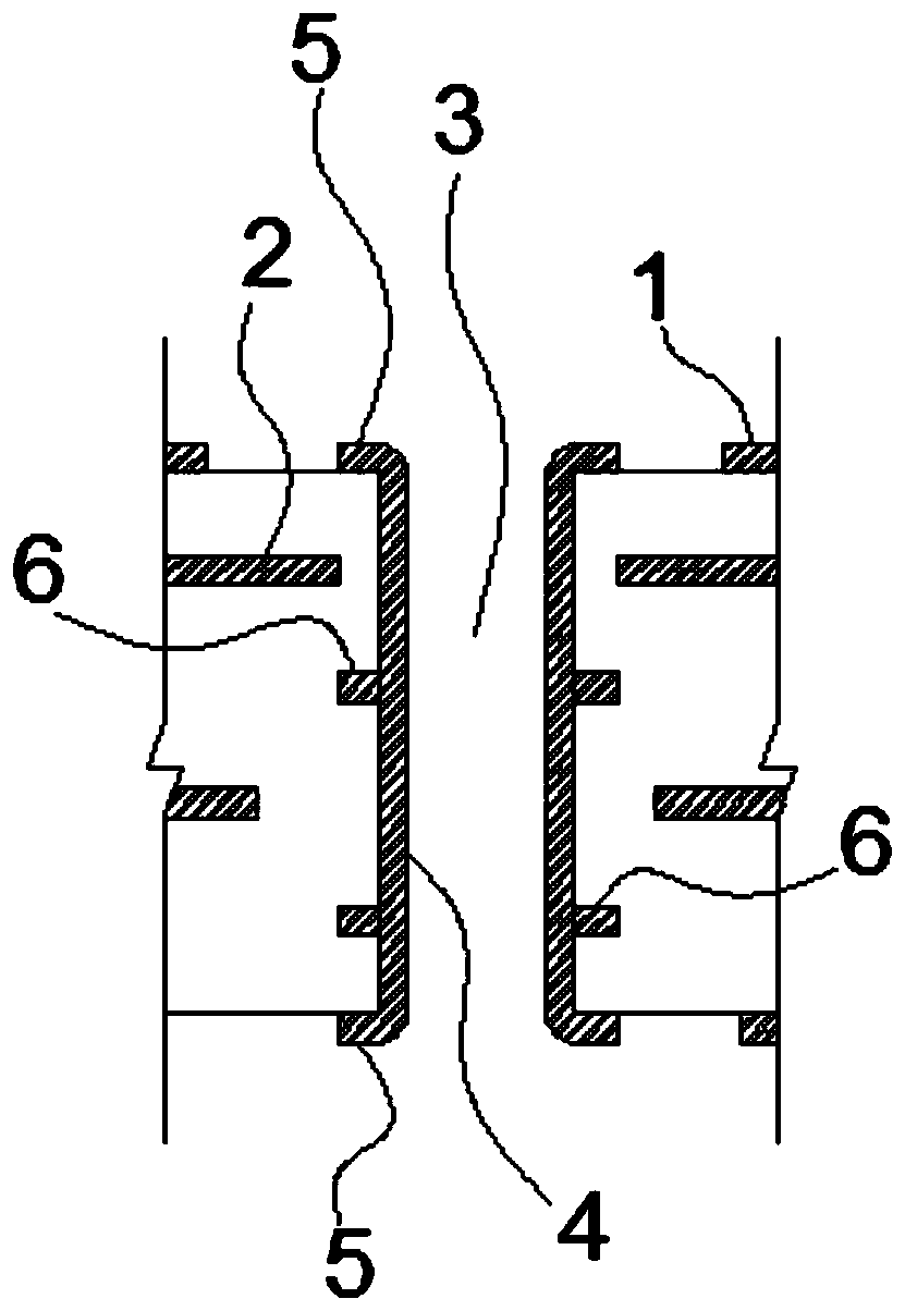
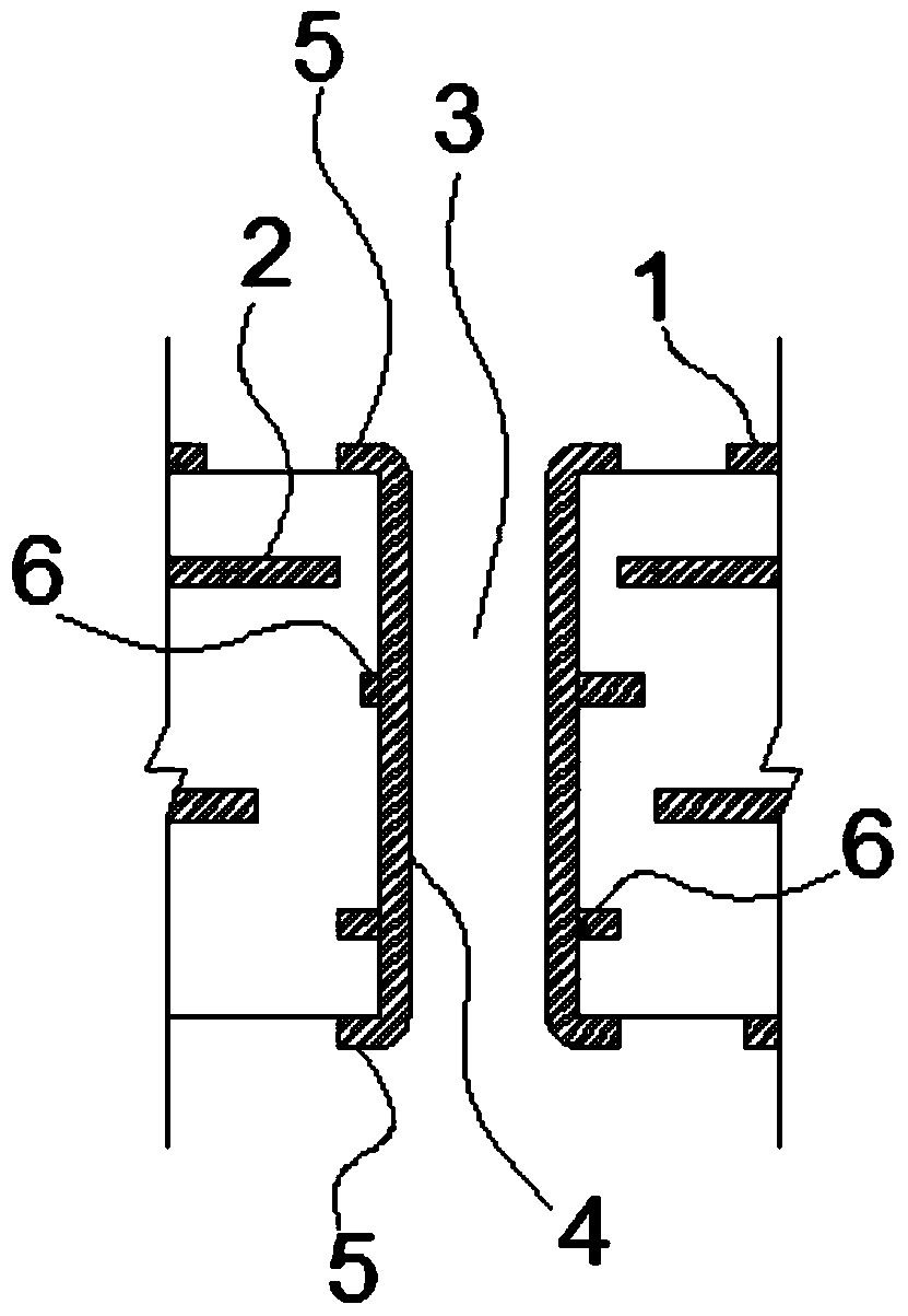
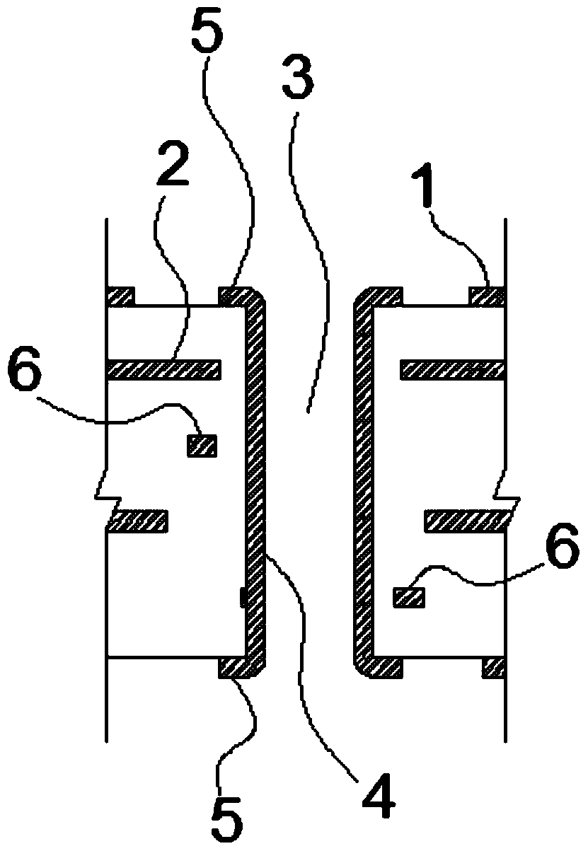
[0020] Embodiment: a kind of multilayer printed circuit board inner layer monitoring structure, the longitudinal stacking structure of the working piece of multilayer printed wiring board has outer layer 1 and multilayer inner layer 2, and the plane layout of the working piece of multilayer printed wiring board is A plurality of single pieces of circuit boards are arranged, and the edge of the working piece has several slicing holes 3, the slicing holes are through holes through the inner layer and the outer layer, and the inner surface of the slicing holes is covered with copper skin 4. The outer layer of the working sheet and the outer periphery of the slicing hole are provided with an outer copper ring 5, the outer copper ring is connected to the copper skin in the slicing hole, and the inner layer of the working sheet is located at the slicing hole. An inner layer copper ring 6 is arranged on the periphery of the hole, and the inner layer copper ring is connected with the c...


PUM


Abstract

The invention discloses an internal layer monitoring structure of a multilayer printed circuit board. The lengthways laminated structure of a working sheet of the multilayer printed circuit board comprises an external layer and multiple internal layers; the plane layout of the working sheet of the multilayer printed circuit board is that multiple circuit board single sheets are arranged; a plurality of sheet-cutting holes are formed in the edge of the working sheet; the sheet-cutting holes are through holes which run through the internal layers and the external layer; the inner surface of each sheet-cutting hole is covered with a copper sheet; the external layer of the working sheet, which is located at the periphery of the sheet-cutting holes, is provided with an external copper ring; the external copper ring is connected with the copper sheet located in each sheet-cutting hole; each internal layer of the working sheet, which is located at the periphery of the sheet-cutting holes, is provided with an internal copper ring; each internal copper ring is connected with the copper sheet in each sheet-cutting hole; the width of each internal copper ring is the maximum acceptable value of the deviation of the internal layers. When internal layer monitoring is needed, the sheet-cutting holes are taken off and cut off by using a sheet punching machine; besides the conventional internal lay data monitoring, whether the internal layers are in poor alignment can be judged through observing whether the sheet-cutting holes are located in the internal copper rings.

Description

technical field [0001] The invention belongs to the field of in-board quality monitoring of printed circuit boards, and in particular relates to a structure of a slicing hole. Background technique [0002] Multi-layer circuit boards are generally produced in joints, and the full-page work sheet generally includes dozens or even hundreds of circuit boards. For example, a memory stick circuit board is generally a work piece composed of 108 memory stick circuit boards. produced simultaneously. In order to assist in the quality control of the inner layer, several slicing holes are generally designed on the edge of the working piece. The slicing hole is a through hole that runs through the working piece. The shape and structure of the slicing hole fully reflect the situation of the circuit board on the working piece. , when it is necessary to monitor the quality of the inner layer, it is necessary to use a punching machine to remove the entire slicing hole from the working sheet...

Claims


Application Information

Patent Timeline
Patent Type & Authority Patents(China)
IPC IPC(8): H05K1/02
CPCH05K1/0269H05K2201/20
Inventor 李泽清
Owner 竞陆电子(昆山)有限公司
Why Eureka
Try Eureka