Circuit board and manufacturing method thereof

A manufacturing method and circuit board technology, applied to printed circuit components, other printed circuit components, electrical connection printed components, etc., can solve the problem of weakening the effect of power filter circuits, inability to accurately control via impedance, and affecting signal rise time, etc. problem, achieve the effect of reducing impedance discontinuity, improving effect and reducing insertion loss

Active Publication Date: 2018-10-19
XIAOMI INC
View PDF3 Cites 0 Cited by
  • Summary
  • Abstract
  • Description
  • Claims
  • Application Information

AI Technical Summary

Problems solved by technology

[0004] In low-frequency circuits, vias have no effect on signal transmission, but in radio-frequency circuits, high-speed circuits, and power circuits, vias will have many adverse effects
First of all, the current technology still cannot accurately control the impedance of the via hole. The via hole will form a discontinuous breakpoint on the trace, causing signal reflection. In addition, the via hole with the same length has greater loss than the microstrip line. Holes have an inevitable impact on high-frequency signals; secondly, the parasitic capacitance generated by vias will affect the rise time of signals, reduce the speed of the circuit, and greatly reduce the signal quality in high-speed circuits; finally, the parasitic inductance will offset the bypass The role of the circuit capacitor, weakening the effect of the power filter circuit

Method used


Image

  • Circuit board and manufacturing method thereof
  • Circuit board and manufacturing method thereof
  • Circuit board and manufacturing method thereof

Examples


Embodiment Construction

[0029] Reference will now be made in detail to the exemplary embodiments, examples of which are illustrated in the accompanying drawings. When the following description refers to the accompanying drawings, the same numerals in different drawings refer to the same or similar elements unless otherwise indicated. The implementations described in the following exemplary examples do not represent all implementations consistent with the present disclosure. Rather, they are merely examples of apparatuses and methods consistent with aspects of the present disclosure as recited in the appended claims.

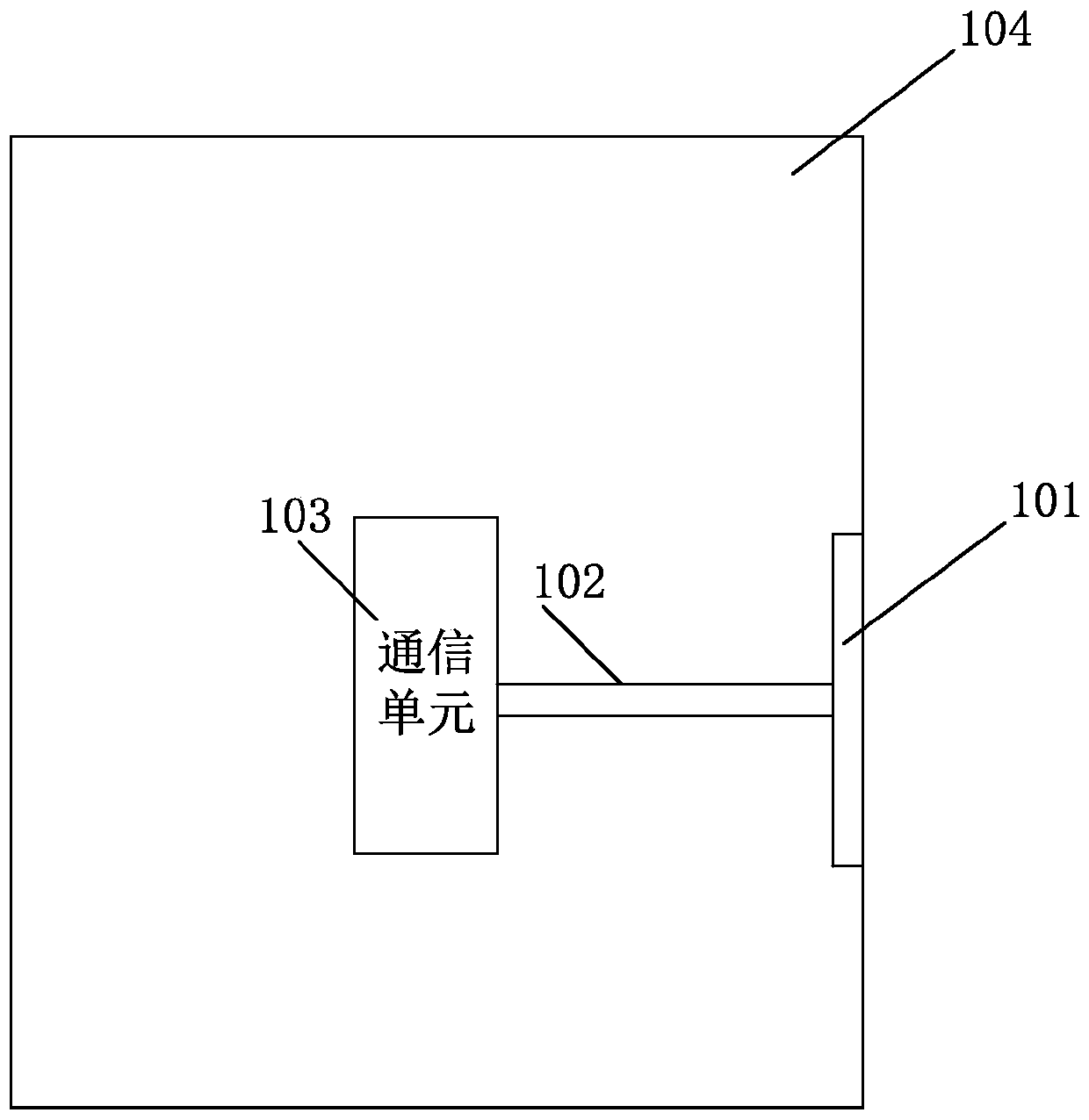
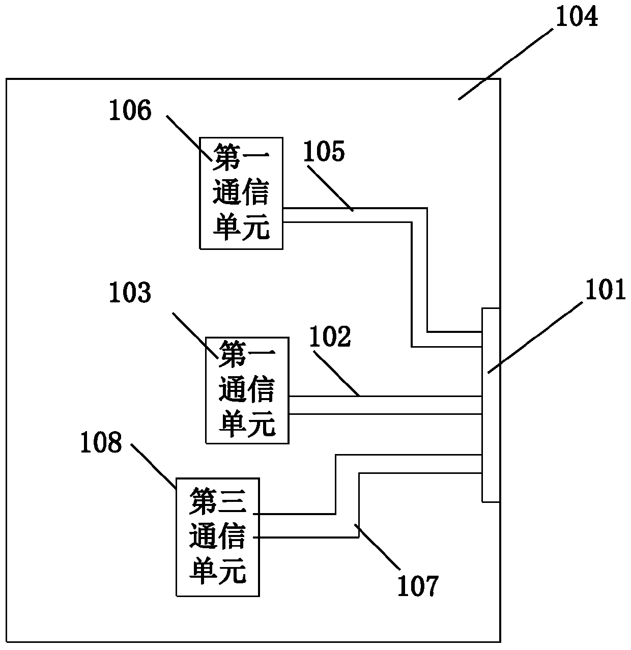
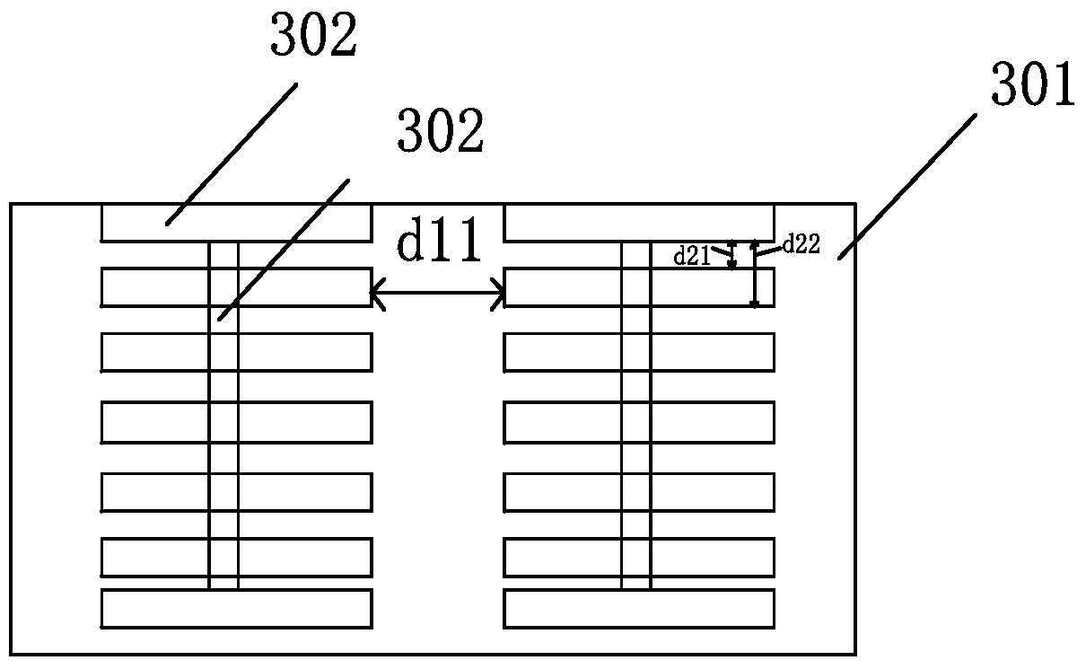
[0030] According to a first aspect of an embodiment of the present disclosure, a circuit board is provided, including a multi-layer signal transmission layer, and the circuit board further includes: a plurality of first signal transmission units disposed on the first signal transmission layer, each first signal transmission unit Including at least one first signal transmission line; a ...


PUM


Abstract

The invention discloses a circuit board and a manufacturing method thereof. The circuit board comprises a first signal transmission layer and a second signal transmission layer. The circuit board also comprises a plurality of first signal transmission units arranged on the first signal transmission layer; a plurality of second signal transmission units arranged on the second signal transmission layer and corresponding to the plurality of first signal transmission units; and edge connection units corresponding to the first signal transmission units, wherein corresponding first signal transmission units and second signal transmission units form electric connection through corresponding connection units; the connection units are divided into at least two rows to form at least two connection layers; in directions parallel with the connection layers, adjacent connection layers form an offset; in the directions perpendicular to the connection layers in the first signal transmission layer, adjacent connection layers are overlapped partially. According to the invention, the signal transmission quality of the circuit board is improved.

Description

technical field [0001] The present disclosure relates to the field of circuit board design, in particular to a circuit board and a manufacturing method thereof. Background technique [0002] The demand for products in the display field in the contemporary market is further developing towards large size, high speed and ultra-high definition. This will inevitably require higher density, higher speed printed circuit boards. [0003] The transmission quality of the signal on the printed circuit board directly affects the performance of the printed circuit board product. In high-speed printed circuit boards, many signals need to be transmitted in multiple signal transmission layers. When signals need to be transmitted in multiple signal transmission layers, vias need to be provided between different signal transmission layers, and signal transmission units located in different signal transmission layers are connected through the vias to continuously transmit signals. [0004] ...

Claims


Application Information

Patent Timeline
Patent Type & Authority Patents(China)
IPC IPC(8): H05K1/11H05K3/40
CPCH05K1/11H05K3/40H05K2201/20H05K2203/0502
Inventor 曾超张良飞韦钰达
Owner XIAOMI INC
Why Eureka
Try Eureka