
Method for manufacturing silicon carbide MOSFET

A manufacturing method and technology of silicon carbide, which are applied in semiconductor/solid-state device manufacturing, electrical components, circuits, etc., can solve the problems of poor threshold voltage adjustment capability, long gate signal delay time, and high polysilicon resistivity, so as to improve the adjustment capability. , the effect of reducing the delay time of the gate signal

Inactive Publication Date: 2015-11-18
ZHUZHOU CSR TIMES ELECTRIC CO LTD
View PDF4 Cites 2 Cited by
  • Summary
  • Abstract
  • Description
  • Claims
  • Application Information

AI Technical Summary

Problems solved by technology

[0003] However, in the process of manufacturing silicon carbide MOSFET power devices using silicon-based semiconductor manufacturing technology, due to the unique properties of silicon carbide, some problems have arisen: at present, the gate electrode of silicon carbide MOSFET power devices uses doped polysilicon, due to carbonization The forbidden band width of silicon is large (3.2eV), while the forbidden band width of polysilicon is small (1.1eV), which makes the doping concentration of the polysilicon gate electrode less able to adjust the threshold voltage of silicon carbide MOSFET. Moreover, due to the resistance of polysilicon The rate is large, and the gate signal delay time is long in large-area silicon carbide MOSFET devices

Method used


Image

  • Method for manufacturing silicon carbide MOSFET
  • Method for manufacturing silicon carbide MOSFET
  • Method for manufacturing silicon carbide MOSFET

Examples


Embodiment Construction

[0025] The technical solutions in the embodiments of the present invention will be clearly and completely described below in conjunction with the accompanying drawings in the embodiments of the present invention. Obviously, the described embodiments are only a part of the embodiments of the present invention, rather than all the embodiments. Based on the embodiments of the present invention, all other embodiments obtained by those of ordinary skill in the art without creative work shall fall within the protection scope of the present invention.

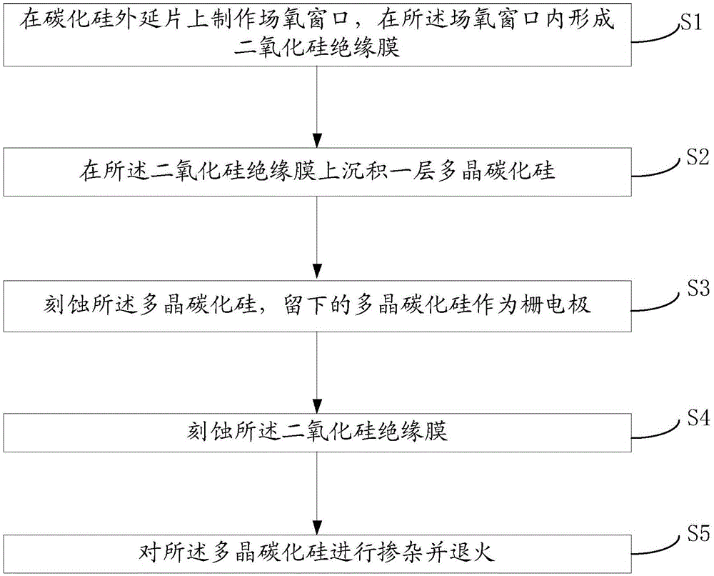
[0026] The manufacturing method of a silicon carbide MOSFET provided by the embodiment of the application is as follows figure 1 As shown, figure 1 This is a schematic diagram of a method for manufacturing a silicon carbide MOSFET provided by an embodiment of this application. The method includes the steps:

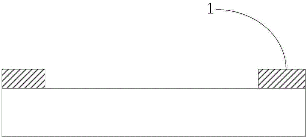
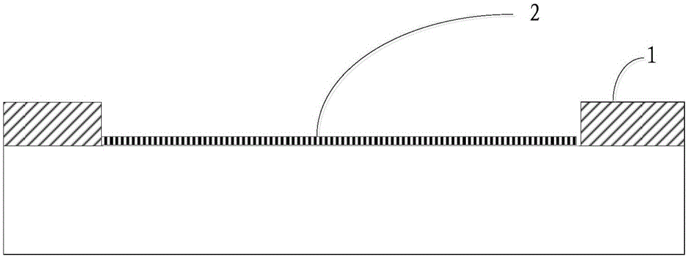
[0027] S1: forming a field oxygen window on the silicon carbide epitaxial wafer, and forming a silicon dioxide insulating film in th...


PUM


Abstract

The present invention discloses a method for manufacturing a silicon carbide MOSFET. The method comprises the steps of making a field oxide window on a silicon carbide epitaxial piece and forming a silicon dioxide insulating film in the field oxide window, depositing a layer of polycrystalline silicon carbide on the silicon dioxide insulating film, etching the polycrystalline silicon carbide and taking the remaining polycrystalline silicon carbide as a gate electrode, etching the silicon dioxide insulating film, and doping the polycrystalline silicon carbide and carrying out annealing. Due to the above methods, the deposed polycrystalline silicon carbide is used to make the gate electrode of the silicon carbide MOSFET, thus the adjustment ability of device threshold voltage can be improved, and the gate signal delay time can be reduced.

Description

Technical field [0001] The invention relates to the technical field of semiconductor device manufacturing, in particular to a method for manufacturing a silicon carbide MOSFET. Background technique [0002] Silicon carbide, as a representative of the third-generation semiconductor material, has outstanding advantages such as wide band gap, high saturation drift speed, high thermal conductivity and high critical breakdown electric field. It is particularly suitable for making high-power, high-pressure, high-temperature and radiation-resistant electronic devices. Compared with other wide-bandgap semiconductors, silicon carbide is the only semiconductor material that can grow a silicon dioxide layer on its surface by thermal oxidation, which means that silicon carbide is used to make high-power metal-oxide semiconductor field effect transistors (MOSFET) And an ideal material for insulated gate bipolar transistors (IGBT). [0003] However, in the process of using silicon-based semicon...

Claims


Application Information

Patent Timeline
Patent Type & Authority Applications(China)
IPC IPC(8): H01L21/336H01L29/78H01L29/43H01L29/423
CPCH01L29/66477H01L29/42372H01L29/43H01L29/78
Inventor 陈喜明邵云李诚瞻赵艳黎高云斌丁荣军
Owner ZHUZHOU CSR TIMES ELECTRIC CO LTD
Learn More