


Quick Research
Generate reliable direction feasibility study reports for your R&D in just a few steps.

Technical Q&A
Discover and master advanced knowledge NOW. Basics, ideas, possibilities, all at once.

Find Solutions
As an expert in R&D theories, this can generate solutions to your technical problems instantly.

Evaluate Feasibility
Analyze your overall solution with one click, know your potential R&D risks in advance.

Monitor Landscape
Get weekly tech updates, stay abreast of the latest tech innovations and key insights.
Switch transistor voltage drop holding circuit and application of switch transistor voltage drop holding circuit in lithium battery protection circuit
A technology of switching transistors and holding circuits, applied in lithium battery charge and discharge protection circuits, in the field of switching transistor voltage drop holding circuits, can solve problems such as failure to reach the opening voltage value and failure of lithium battery protection control circuits to receive power, etc., to achieve The effect of simple structure
- Summary
- Abstract
- Description
- Claims
- Application Information
AI Technical Summary
Problems solved by technology
Method used
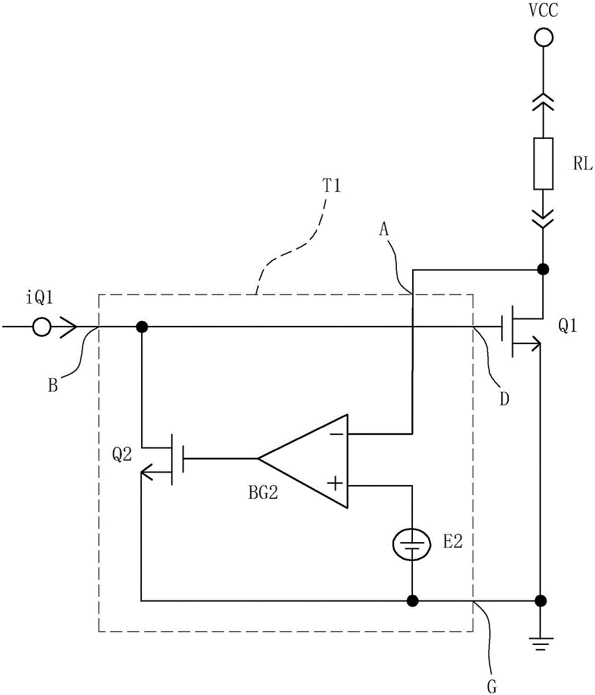
Image

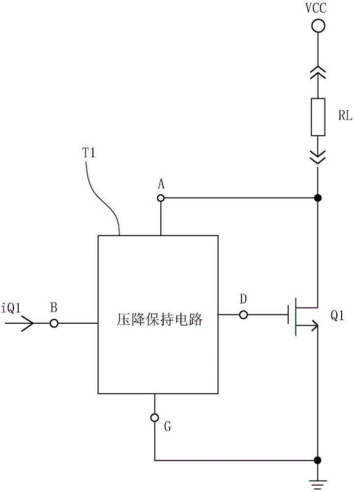
Examples
Embodiment 1
[0034] Embodiment one, such as figure 2 , image 3 Shown:
[0035] The switching transistor voltage drop holding circuit T1 of the first embodiment is specifically: including an N-channel second field effect transistor Q2 and a second comparator BG2, wherein the negative input terminal of the second comparator BG2 is connected to the first field effect transistor The drain of Q1 is connected, the positive input terminal of the second comparator BG2 is grounded after passing through the second reference voltage E2, the source of the first field effect transistor Q1 is grounded; the output terminal of the second comparator BG2 is connected to the second field effect transistor Q2 The gate of the second field effect transistor Q2 is connected to the gate of the first field effect transistor Q1, and the other is connected to the driving signal iQ1 of the first field effect transistor Q1, and the drain of the second field effect transistor Q2 is connected to the gate of the first...
Embodiment 2
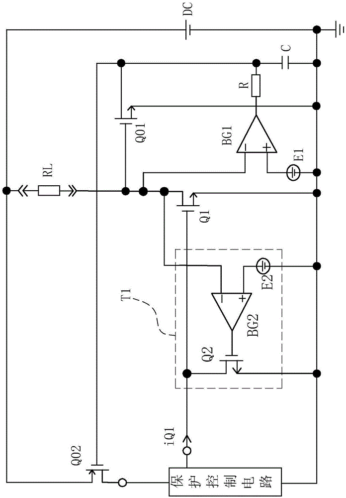
[0044] Embodiment two, such as Figure 4 , Figure 5 Shown:
[0045] The voltage drop holding circuit T1 of the second embodiment is specifically: including a P-channel third field effect transistor Q3 and a third comparator BG3, wherein the negative input terminal of the third comparator BG3 is connected to the first field effect transistor Q1 The drains are connected, the positive input terminal of the third comparator BG3 is grounded after passing through the third reference voltage E3, the source of the first field effect transistor Q1 is grounded; the output terminal of the third comparator BG3 is connected to the gate of the third field effect transistor Q3 The source of the third field effect transistor Q3 is connected to the driving signal iQ1 of the first field effect transistor Q1, and the drain of the third field effect transistor Q3 is connected to the gate of the first field effect transistor Q1.
[0046] Figure 5 It is the application of the switching transis...
PUM
 Abstract
Description
Claims
Application Information
 - R&D Engineer
- R&D Manager
- IP Professional
- Industry Leading Data Capabilities
- Powerful AI technology
- Patent DNA Extraction
Browse by: Latest US Patents, China's latest patents, Technical Efficacy Thesaurus, Application Domain, Technology Topic, Popular Technical Reports.
© 2024 PatSnap. All rights reserved.Legal|Privacy policy|Modern Slavery Act Transparency Statement|Sitemap|About US| Contact US: help@patsnap.com