Polycrystal minority carrier lifetime detection back lineation measuring tool
A low-lifetime and post-testing technology, applied in the direction of manufacturing tools and workshop equipment, can solve the problems of heavy workload, reduced work efficiency, time-consuming and labor-intensive operation, etc., and achieve the effect of reasonable structure, improved work efficiency, and low requirements for operators
- Summary
- Abstract
- Description
- Claims
- Application Information
AI Technical Summary
Problems solved by technology
Method used
Image
Examples
Embodiment 1
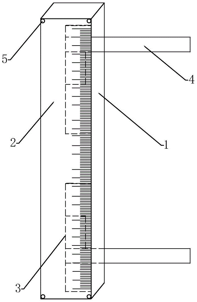
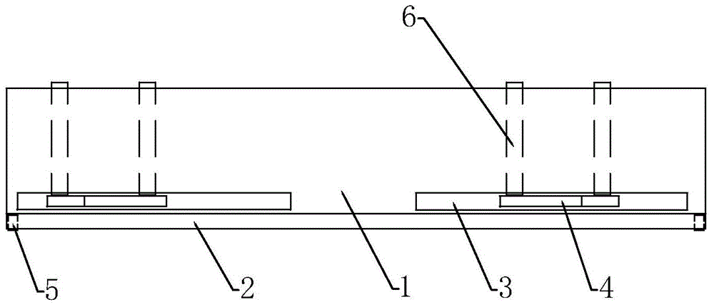
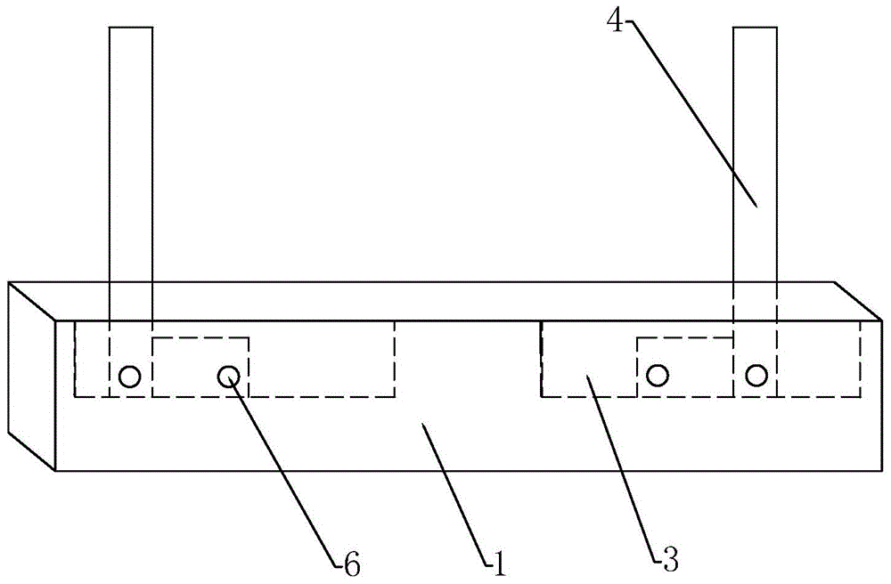
[0018] as attached Figure 1-3 As shown, the polycrystalline minority-carrier life-span test scribe measuring tool includes a wooden base 1, and a scale 2 attached to the wooden base 1 is connected to the front end of the wooden base 1, and the upper and lower ends of the scale 2 are connected One side of the front part of the corresponding wooden base 1 is respectively provided with a groove 3, and a square 4 is respectively slid up and down in the groove 3; There is a first fastening screw 5 penetrating into the fixed square 4 in the groove.
[0019] The four corners of the scale 2 are respectively provided with a second fastening screw 6 , and the scale 2 is fixedly connected with the front end of the wooden base 1 through the second fastening screw 5 .
Embodiment 2
[0021] as attached Figure 4-5 As shown, it is another embodiment of the present invention. The difference between the scribing measuring tool after the minority carrier lifetime detection and the embodiment 1 is that the back of the scale 2 and the front end of the wooden base 1 are bonded and fixed by an adhesive 7. even.
[0022] Hereinafter, taking a certain squared silicon ingot as an example, the method of using the scribing measuring tool after polycrystalline minority carrier lifetime testing in Embodiment 1 and Embodiment 2 of the present invention is described. Divide the silicon ingot into 5*5 pieces of silicon blocks with a size of 156*156 in total, and divide them into A area (9 blocks) / B area (12 blocks) / C (4 blocks) according to the position of the silicon block in the silicon ingot. block), select each silicon block in each area for minority carrier lifetime detection, and mark the head and tail unqualified areas according to the test results of silicon blocks...
PUM
 Abstract
Description
Claims
Application Information
 - R&D
- Intellectual Property
- Life Sciences
- Materials
- Tech Scout
- Unparalleled Data Quality
- Higher Quality Content
- 60% Fewer Hallucinations
Browse by: Latest US Patents, China's latest patents, Technical Efficacy Thesaurus, Application Domain, Technology Topic, Popular Technical Reports.
© 2025 PatSnap. All rights reserved.Legal|Privacy policy|Modern Slavery Act Transparency Statement|Sitemap|About US| Contact US: help@patsnap.com


