Device and method for measuring frequency response of optical device
A frequency response, measuring light technology, applied in transmission monitoring/testing/fault measurement systems, etc., can solve problems such as multi-dimensional measurement of optical devices, and achieve the effect of ensuring measurement accuracy and bandwidth, optimizing the conflicting relationship, and ensuring measurement speed.
- Summary
- Abstract
- Description
- Claims
- Application Information
AI Technical Summary
Problems solved by technology
Method used
Image

Examples
Embodiment 1
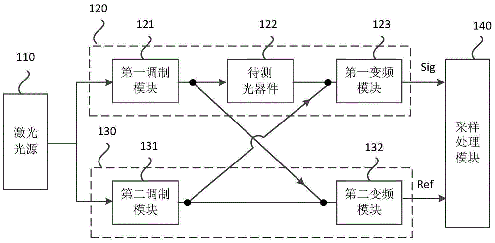
[0063] This embodiment provides a device for measuring the frequency response of an optical device. figure 1 Schematic diagram of the structure of the device. The device includes a laser light source 110 , a detection optical path 120 , a reference optical path 130 and a sampling processing module 140 .
[0064] Wherein, the laser light source 110 is used to generate a continuous laser carrier. The detection optical circuit 120 modulates the laser carrier to generate a first optical frequency comb, so that the first optical frequency comb passes through the optical device under test to obtain a detection optical comb, so as to record the amplitude-frequency response and phase-frequency response of the optical device under test in the detection optical comb On the comb teeth of the detection optical path 120, the frequency conversion of the detection optical comb is also converted into a baseband detection signal Sig. The reference optical path 130 modulates the laser carrier...
Embodiment 2
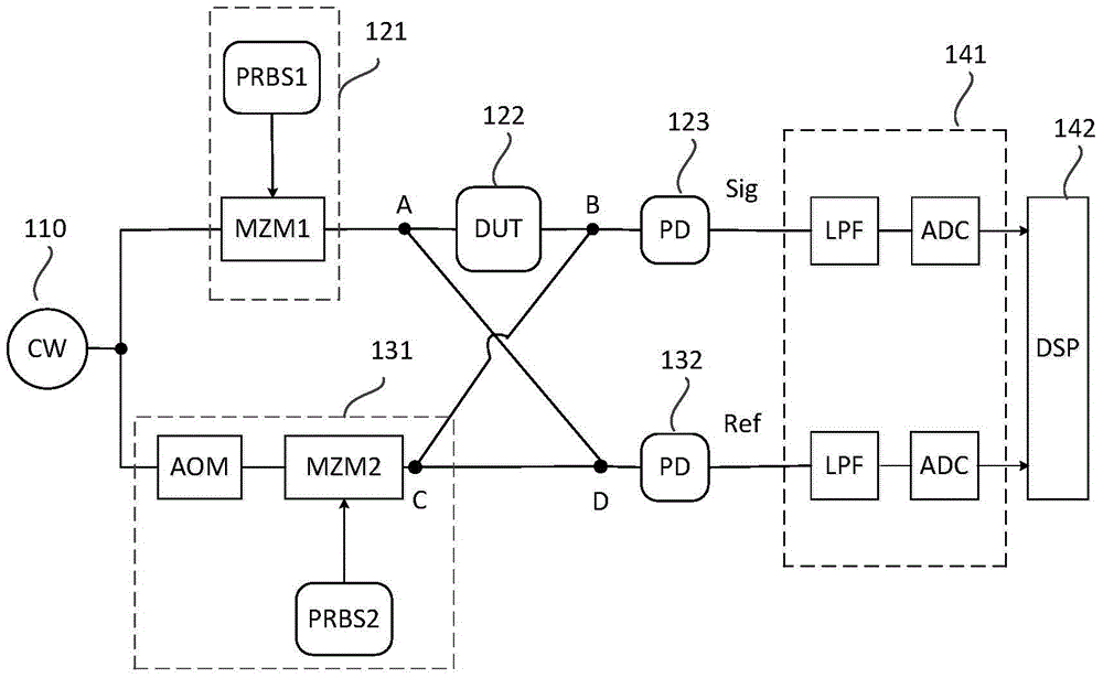
[0076] This example is for figure 1 The individual components of the shown device are described in detail. image 3 is a schematic structural diagram of the device used to measure the frequency response of the optical device in this embodiment. image 3 and figure 1 The same reference numerals are used for the same components.
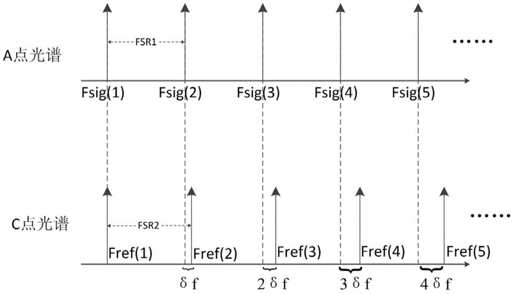
[0077] It should be noted that since the optical frequency response of the optical device under test is recorded on the comb teeth of the optical frequency comb, it is necessary to calculate the information recorded on each comb tooth in the post-processing process. If the detection bandwidth is increased without increasing the amount of calculation, the interval between comb teeth will inevitably increase, resulting in a decrease in detection accuracy. like image 3 As shown, in this implementation, the PRBS code is used to modulate the continuous laser source to generate an optical frequency comb, so as to flexibly set the detection accuracy and ...
Embodiment 3
[0091] This embodiment provides a method for measuring the frequency response of an optical device. like Figure 5 As shown, firstly a continuous laser carrier is generated (step S501). The laser carrier is modulated to generate a first optical frequency comb (step S502), specifically, the laser carrier is modulated to generate a first optical frequency comb with a first frequency interval. Passing the first optical frequency comb through the optical device under test to obtain a detection optical comb (step S503 ), so as to record the amplitude-frequency response and phase-frequency response of the optical device under test on the teeth of the detection optical comb.
[0092] Modulating the laser carrier to generate a second optical frequency comb (step S504), specifically, shifting the frequency of the laser carrier, and modulating to generate a second optical frequency comb with a second frequency interval, and the first frequency interval It is different from the value o...
PUM
 Abstract
Description
Claims
Application Information
 - R&D
- Intellectual Property
- Life Sciences
- Materials
- Tech Scout
- Unparalleled Data Quality
- Higher Quality Content
- 60% Fewer Hallucinations
Browse by: Latest US Patents, China's latest patents, Technical Efficacy Thesaurus, Application Domain, Technology Topic, Popular Technical Reports.
© 2025 PatSnap. All rights reserved.Legal|Privacy policy|Modern Slavery Act Transparency Statement|Sitemap|About US| Contact US: help@patsnap.com