Tungsten film forming method and semiconductor device manufacturing method
A film-forming method and manufacturing method technology, which is applied in semiconductor/solid-state device manufacturing, electrical components, coatings, etc., can solve problems such as difficulty in coping with high step coverage, and achieve the effect of avoiding complicated procedures
- Summary
- Abstract
- Description
- Claims
- Application Information
AI Technical Summary
Problems solved by technology
Method used
Image
Examples
experiment example 1
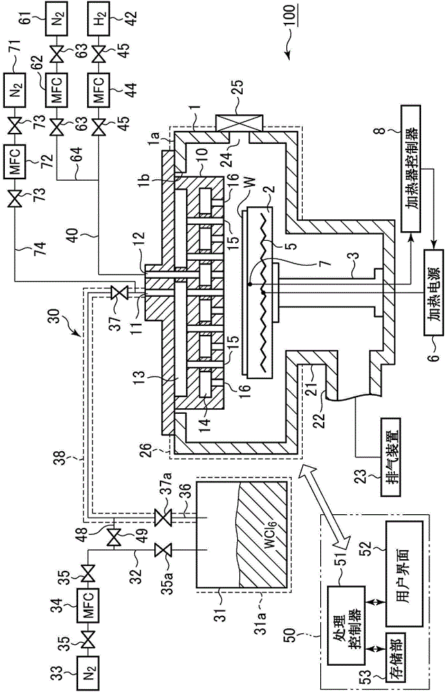
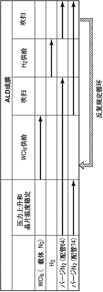
[0111] First, the relationship between the film thickness of the tungsten film and the resistivity of the film is obtained. Here, use figure 1 Tungsten films with various film thicknesses were formed by ALD on a TiN film formed on the surface of a silicon wafer, and the resistivity of each film was measured. The condition at this time is fixed as: Carrier N 2 Gas flow: 500sccm (WCl 6 Flow: 10sccm), H 2 Gas flow: 4500sccm, WCl 6 Time to supply one step: 1.5sec, H 2 The time for one gas supply step: 3 sec, the time for one purge step: 5 sec, the number of cycles: 200 to 1000 times, and the temperature and pressure conditions are the following three conditions of condition A, condition B and condition C.
[0112] [Condition A] Temperature: 500°C, Pressure: 30Torr
[0113] [Condition B] Temperature: 500°C, Pressure: 20Torr
[0114] [Condition C] Temperature: 430°C, Pressure: 30Torr
[0115] exist Figure 6 Shows the results of the above experiments. As shown in the figur...
experiment example 2
[0117] Here, a TiN film was formed as a base film in a hole with a top diameter of 180 nm and an aspect ratio of 60, and a tungsten film was directly formed thereon by ALD to fill the hole. The conditions at this time are: use figure 1 film forming device, wafer temperature: 500°C, chamber pressure: 30Torr, carrier N 2 Gas flow: 500sccm (WCl 6 Flow: 10sccm), H 2 Gas flow: 4500sccm, WCl 6 Time to supply one step: 1.5sec, H 2 Time for one gas supply step: 3 sec, time for one purge step: 5 sec, number of cycles: 500 times.
[0118] exist Figure 7 A SEM photograph of the cross section at this time is shown in . Such as Figure 7 As shown, it was confirmed that the nucleation film was not applied, and a tungsten film was obtained with a good step coverage to the bottom of the hole with a top diameter of 180 nm and an aspect ratio of 60 by one-step film formation.
experiment example 3
[0120] Here, only H is used as reducing gas 2 gas and in H 2 Add NH to the gas 3 The film-forming properties in gas were evaluated. use figure 1 Tungsten film is formed at various temperatures by the ALD method on the TiN film formed on the surface of the silicon wafer. As a condition at this time, for the carrier N 2 Gas flow: 500sccm (WCl 6 Flow: 10sccm), WCl 6 Time for one gas supply step: 1.5sec, H 2 Time for one gas supply step: 3 sec, time for one purge step: 5 sec, number of cycles: 50 to 300 times, when only H is used as reducing gas 2 When the gas is 2000sccm, and in H 2 Add NH to gas 2000sccm 3 When the gas is 25 to 1500 sccm, the tungsten film is formed at a wafer temperature (table surface temperature): 250 to 500°C.
[0121] exist Figure 8 In indicates that only H is used as reducing gas 2 The relationship between the wafer temperature and the film formation rate (per 1 cycle) in the gas, in Figure 9 denoted as reducing gas in H 2 Add NH to the gas...
PUM
| Property | Measurement | Unit |
|---|---|---|
| thickness | aaaaa | aaaaa |
Abstract
Description
Claims
Application Information
 - R&D Engineer
- R&D Manager
- IP Professional
- Industry Leading Data Capabilities
- Powerful AI technology
- Patent DNA Extraction
Browse by: Latest US Patents, China's latest patents, Technical Efficacy Thesaurus, Application Domain, Technology Topic, Popular Technical Reports.
© 2024 PatSnap. All rights reserved.Legal|Privacy policy|Modern Slavery Act Transparency Statement|Sitemap|About US| Contact US: help@patsnap.com


