Transport systems, reaction chambers and semiconductor processing equipment

A technology of a reaction chamber and a transmission system, applied in the field of semiconductor processing, can solve the problems of easy occurrence of eddy current, poor process quality, easy diffusion, etc., and achieve the effects of improving uniformity, improving yield, and improving process quality

Active Publication Date: 2018-01-19
BEIJING NAURA MICROELECTRONICS EQUIP CO LTD
View PDF5 Cites 0 Cited by
  • Summary
  • Abstract
  • Description
  • Claims
  • Application Information

AI Technical Summary

Problems solved by technology

[0005] However, the following problems inevitably exist in the actual application of the above-mentioned silicon epitaxial equipment, that is: since the gate valve 15 is arranged at the port of the transfer device 12 that is not connected with the reaction chamber 10, the transfer channel 14 is always in the process. It communicates with the reaction chamber 10, and since a plurality of gas inlets 12a for delivering the process gas to the central area of ​​the reaction chamber 10 are close to the transmission channel 14, this makes it easy for the process gas delivered to the central area of ​​the reaction chamber 10 to diffuse to In the transmission channel 14, the flow rate of the process gas in the central region of the reaction chamber 10 is likely to be reduced, and the vortex phenomenon is prone to occur, such as image 3 and Figure 4 As shown, resulting in poor uniformity of the process gas in the reaction chamber, resulting in poor process quality

Method used


Image

  • Transport systems, reaction chambers and semiconductor processing equipment
  • Transport systems, reaction chambers and semiconductor processing equipment
  • Transport systems, reaction chambers and semiconductor processing equipment

Examples


Embodiment Construction

[0034] In order for those skilled in the art to better understand the technical solution of the present invention, the transmission system, reaction chamber and semiconductor processing equipment provided by the present invention will be described in detail below with reference to the accompanying drawings.

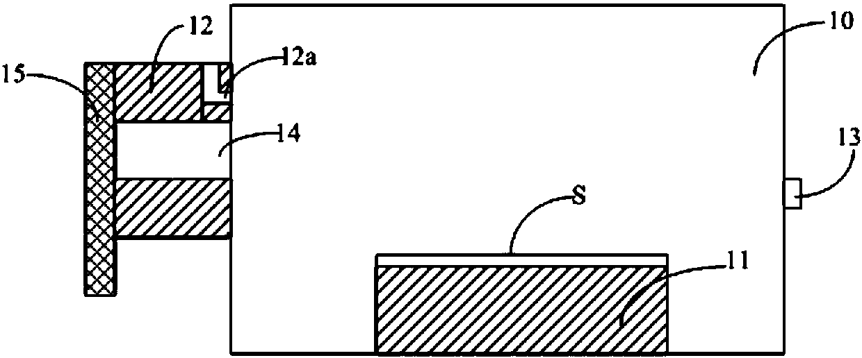
[0035] Figure 5 It is a schematic structural diagram of the transmission system provided by the first embodiment of the present invention. see Figure 5 , the transmission system provided by the present invention includes a transmission device 20 and a gate valve 21, a transmission channel 201 communicating with the reaction chamber is provided on the transmission device, the transmission device 20 can be specifically a flange, and the transmission channel 201 is used as a processed The workpiece moves into or out of the passage of the reaction chamber, and the gate valve 21 is used to open or close the transfer channel 201, and the gate valve 21 is arranged at the port...


PUM


Abstract

The invention provides a conveying system, a reaction chamber and semiconductor processing equipment. The conveying system comprises a conveying device and a gate. The conveying device is provided with a conveying channel which is communicated with the reaction chamber. The conveying channel is used as the channel for conveying processed workpieces into or out of the reaction chamber. The gate is used for opening or closing the conveying channel. The gate is arranged at the end, which is communicated with the reaction chamber, of the conveying channel. Furthermore the gate opens or closes the conveying channel in an overturning manner. The conveying system provided by the invention can prevent diffusion of process gas into the conveying channel, thereby preventing an eddy phenomenon of the process gas at the central area of the reaction chamber caused by flow speed reduction, improving distribution uniformity of the process gas in the reaction chamber and furthermore improving process quality.

Description

technical field [0001] The invention belongs to the technical field of semiconductor processing, and in particular relates to a transmission system, a reaction chamber and semiconductor processing equipment. Background technique [0002] Silicon epitaxial equipment is used to produce silicon epitaxial wafers. Its working principle is as follows: transport silicon compounds to high temperature (>1100°C) substrates, and use hydrogen (H 2 ) to precipitate silicon on the substrate through a reduction reaction. In practical applications, in order to prevent the external environment from affecting the internal environment of the reaction chamber, thereby affecting the process quality, the reaction chamber is usually sealed during the process. [0003] figure 1 It is a schematic structural diagram of an existing silicon epitaxial equipment. figure 2 for figure 1 The left side view of the silicon epitaxial equipment is shown. Please also refer to figure 1 and figure 2 , ...

Claims


Application Information

Patent Timeline
Patent Type & Authority Patents(China)
IPC IPC(8): H01L21/677H01L21/205
CPCH01L21/02365H01L21/67742H01L21/67763
Inventor 张慧吴军
Owner BEIJING NAURA MICROELECTRONICS EQUIP CO LTD
Why Eureka
Try Eureka