A kind of manufacturing method of germanium layer and semiconductor device

A manufacturing method and semiconductor technology, applied in semiconductor/solid-state device manufacturing, electrical components, circuits, etc., can solve problems affecting device performance, failure, etc., to reduce the number of particle defects, improve particle defects, and improve device performance and device integration. The effect of pass rate

Active Publication Date: 2017-09-29
SHANGHAI HUAHONG GRACE SEMICON MFG CORP
View PDF6 Cites 0 Cited by
  • Summary
  • Abstract
  • Description
  • Claims
  • Application Information

AI Technical Summary

Problems solved by technology

This kind of deposition defect has a certain height and becomes a suspended structure on the surface of the MEMS wafer. It may cause the top of the MEMS wafer to be in direct electrical contact with the ASIC wafer after the bonding of the MEMS wafer and the ASIC wafer, resulting in failure and impact. Device performance

Method used


Image

  • A kind of manufacturing method of germanium layer and semiconductor device
  • A kind of manufacturing method of germanium layer and semiconductor device
  • A kind of manufacturing method of germanium layer and semiconductor device

Examples


Embodiment Construction

[0032] In order to make the purpose and features of the present invention more obvious and understandable, the specific implementation of the present invention will be further described below in conjunction with the accompanying drawings. However, the present invention can be implemented in different forms and should not be limited to the described embodiments.

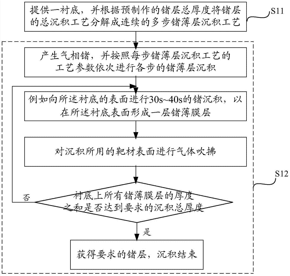
[0033] Please refer to figure 1 , the present invention proposes a kind of preparation method of germanium layer, comprises:

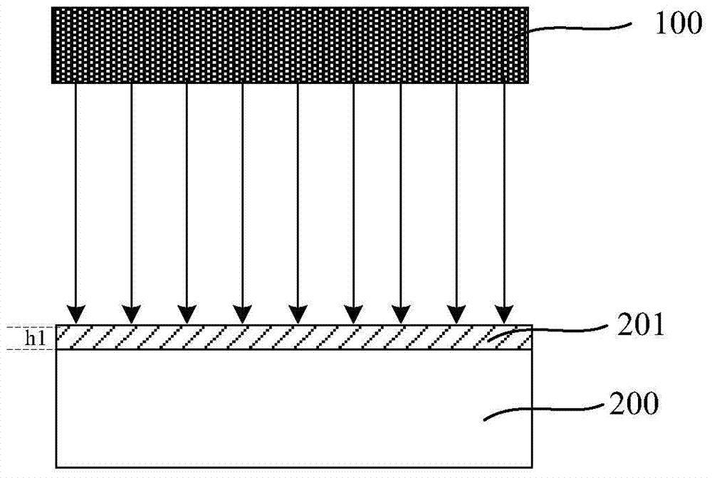
[0034] S11, providing a substrate, and decomposing the total deposition process of the germanium layer into continuous multi-step germanium thin layer deposition processes according to the total thickness of the prefabricated germanium layer;

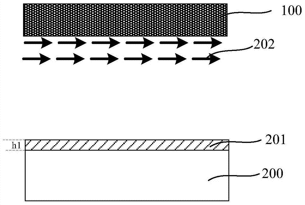
[0035] S12, according to the process parameters of each step of germanium thin layer deposition process, physical vapor deposition of each germanium thin layer in turn on the substrate, and after the last step of germanium thin layer deposition, blowing...


PUM

PropertyMeasurementUnit
electrical resistivityaaaaaaaaaa

Abstract

The invention provides methods for manufacturing a germanium layer and a semiconductor device, and the method for manufacturing the germanium layer comprises the steps: dividing one-step growth, consuming longer time, of a germanium PVD into multi-step growth, consuming shorter time, of the germanium PVD, wherein the sum of thicknesses of deposited germanium at all steps is the required total thickness of the germanium layer, thereby breaking a continuous aggregation process of charges on the surface of a target material; adding a step of large-flow high-pressure air blowing after each divided step of deposition, so as to blow away the charges accumulated on the surface of the target material, thereby reducing the phenomena of arc discharge between the target material and a plasma gun, protecting the target material from being melt partially, reducing the number of spattered particles falling onto a deposition surface after the target material is melt, and finally reducing the defect rate of particles on a deposited germanium layer surface remarkably on the basis of maintaining the total deposition thickness of the germanium layer. The method for manufacturing the semiconductor device employs the method for manufacturing the germanium layer, and improves the performance of the device and the integration qualified rate of the device.

Description

technical field [0001] The invention relates to the field of semiconductor manufacturing, in particular to a method for manufacturing a germanium layer and a semiconductor device. Background technique [0002] Intelligent network terminals such as smartphones and tablet computers have gradually become the necessary communication tools and platforms for handling affairs that people carry with them. As a result, various micro sensors have begun to enter these intelligent network terminals. Integrating more functions, the miniaturization of sensors based on MEMS (Micro-Electro-Mechanical System) technology has become one of the focuses of major companies and related researchers. [0003] At present, integrated circuits (ICs) have achieved wafer-level packaging. On the basis of referring to the wafer-level packaging technology of integrated circuits, a technical solution for the wafer-level packaging process of MEMS devices is proposed for the characteristics of MEMS devices. Sp...

Claims


Application Information

Patent Timeline
Patent Type & Authority Patents(China)
IPC IPC(8): H01L21/203
CPCH01L21/2033
Inventor 赵波
Owner SHANGHAI HUAHONG GRACE SEMICON MFG CORP
Why Eureka
Try Eureka