
Amplification circuit

A technology of amplifying circuit and amplifying stage, which is applied in the direction of differential amplifier, DC coupled DC amplifier, etc., can solve the problems of slow response, high-frequency expansion of difficult frequency band, gain reduction, etc., and achieve the effect of high-speed operation

Active Publication Date: 2015-08-05
ALPS ALPINE CO LTD
View PDF8 Cites 5 Cited by
  • Summary
  • Abstract
  • Description
  • Claims
  • Application Information

AI Technical Summary

Problems solved by technology

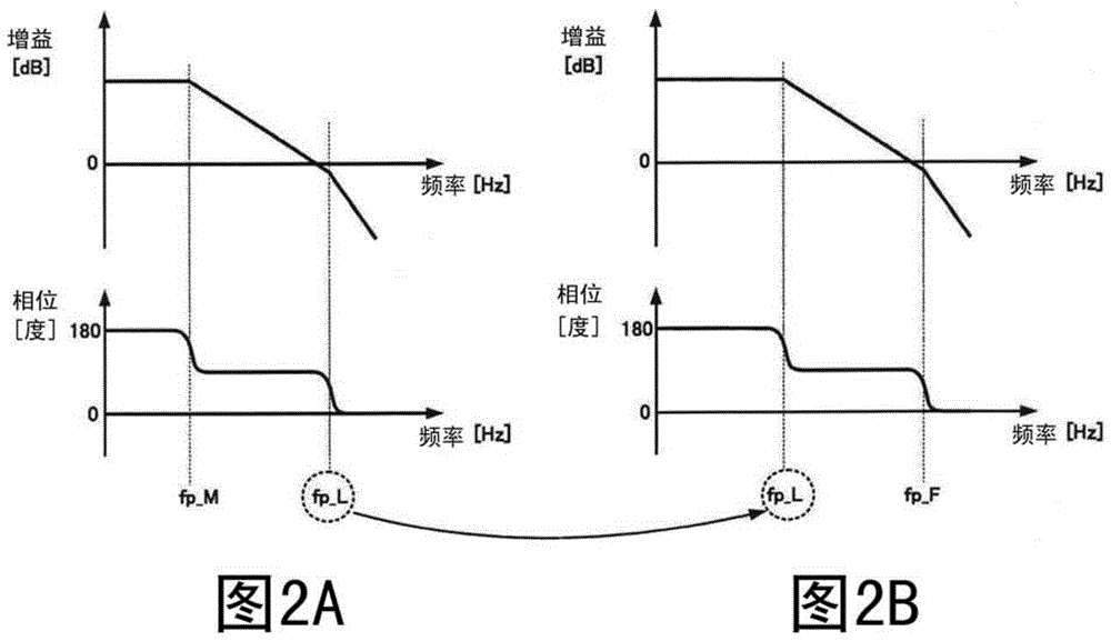
[0011] in having Figure 7 In the conventional operational amplifier with the transfer characteristics shown above, since the upper limit of the frequency band is determined by the pole frequency fp_L caused by the load capacitance and output resistance, there is a problem that it is difficult to expand the frequency band to high frequencies.
[0012] In addition, when the pole frequency fp_L is at a low position, to ensure the stability of the system only by setting the pole frequency fp_M of the phase compensation circuit, the pole frequency fp_M must be lowered, resulting in a significantly slower response
In order to avoid this situation, when the transconductance gm of the MOS transistors Q101 and Q102 constituting the differential pair is reduced to reduce the gain, there is a problem that the input noise becomes larger.

Method used


Image

  • Amplification circuit
  • Amplification circuit
  • Amplification circuit

Examples


Embodiment Construction

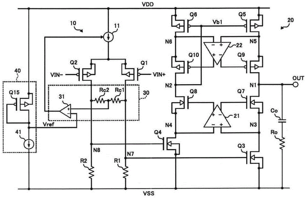
[0032] figure 1 It is a figure which shows an example of the structure of the amplifier circuit which concerns on embodiment of this invention.

[0033] figure 1 The illustrated amplifier circuit has a first amplifier stage 10, a second amplifier stage 20, a common mode feedback unit 30, a reference voltage generator 40, an output capacitor Co, and an output resistor Ro.

[0034] The first amplifier stage 10 is a circuit that amplifies the input differential signal (VIN+, VIN-). figure 1 In the example shown in FIG. 1 , there are a pair of first transistor Q1 and second transistor Q2 constituting a differential pair, a constant current source 11, and resistors R1 and R2. The first transistor Q1 and the second transistor Q2 are P-type MOS transistors.

[0035] One of the differential signals (input signal VIN+) is input to the gate of the first transistor Q1, and the other of the differential signals (input signal VIN−) is input to the gate of the second transistor Q2.

...


PUM


Abstract

The invention provides an amplification circuit which can act in a high speed during connection with a capacitive load. A second amplification stage 20 has a large output resistance. A pole frequency fp_L caused by the output resistance and an output capacitance (a capacitor C0) becomes the lowest pole frequency in a transfer function. When the amplification circuit is compared with a previous amplification circuit wherein the upper limit of a frequency band is limited by a pole frequency fp_L caused by output resistance and output capacitance, the pole frequency limiting the upper limit of a frequency band is raised, and so the lowest pole frequency in the transfer function can be raised to a higher frequency.

Description

technical field [0001] The present invention relates to an amplifying circuit for amplifying a signal output from a sensor, etc., and particularly relates to an amplifying circuit for driving a capacitive load. Background technique [0002] Capacitive sensor elements used in humidity sensors, acceleration sensors, etc. are elements whose electrostatic capacitance changes according to physical quantities, and the change in electrostatic capacitance is generally converted into an electrical signal using an electrostatic capacitance-voltage conversion circuit (also called a CV conversion circuit). . [0003] Figure 5A ~ Figure 5E is a diagram showing an example of a sensor device using a capacitive sensor element. Figure 5A A general configuration of a CV conversion circuit that converts the capacitance of a capacitive sensor element into an electrical signal is shown. Figure 5B and Figure 5C The waveforms of the driving voltages VP1 and VP2 of the capacitive sensor elem...

Claims


Application Information

Patent Timeline
IPC IPC(8): H03F3/45
Inventor 筱井洁
Owner ALPS ALPINE CO LTD
Learn More