A kind of photoconductive ultraviolet detector and its manufacturing method

A technology of an ultraviolet detector and a manufacturing method, which is applied in the field of optoelectronics, can solve the problems of a small effective light-receiving area of ​​an ultraviolet-sensitive film, and achieve the effects of increasing the effective light-receiving area and improving device performance.

Active Publication Date: 2018-07-06
SHANGHAI INST OF MICROSYSTEM & INFORMATION TECH CHINESE ACAD OF SCI
View PDF5 Cites 0 Cited by
  • Summary
  • Abstract
  • Description
  • Claims
  • Application Information

AI Technical Summary

Problems solved by technology

[0004] In view of the shortcomings of the prior art described above, the purpose of the present invention is to provide a photoconductive ultraviolet detector and its manufacturing method, which is used to solve the problem that the effective light-receiving area of ​​the ultraviolet-sensitive film in the prior art is small

Method used


Image

  • A kind of photoconductive ultraviolet detector and its manufacturing method
  • A kind of photoconductive ultraviolet detector and its manufacturing method
  • A kind of photoconductive ultraviolet detector and its manufacturing method

Examples


Embodiment Construction

[0030] The following describes the implementation of the present invention through specific specific examples, and those skilled in the art can easily understand other advantages and effects of the present invention from the content disclosed in this specification. The present invention can also be implemented or applied through other different specific embodiments, and various details in this specification can also be modified or changed based on different viewpoints and applications without departing from the spirit of the present invention.

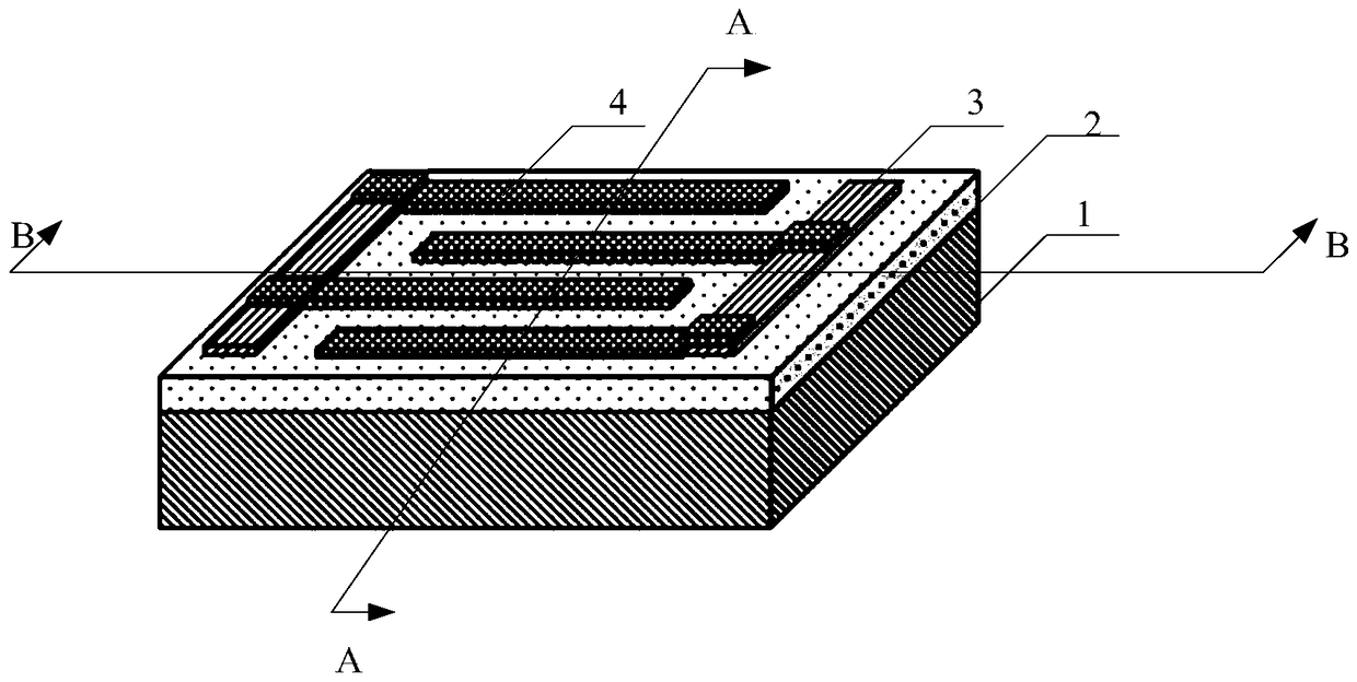
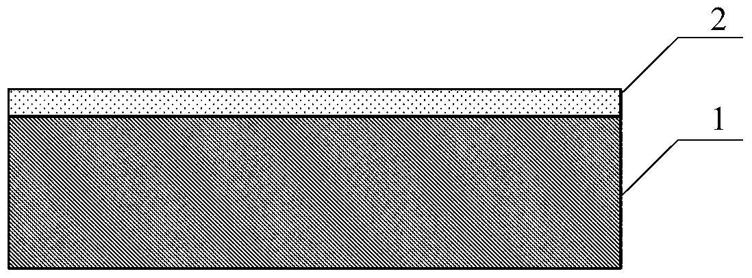
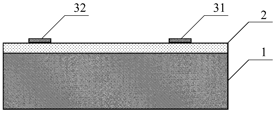
[0031] Please refer to the attached picture. It should be noted that the diagrams provided in this embodiment only illustrate the basic idea of ​​the present invention in a schematic manner. The figures only show the components related to the present invention instead of the number, shape, and shape of the components in actual implementation. For size drawing, the type, quantity, and proportion of each component can be changed at will dur...


PUM

PropertyMeasurementUnit
electron mobilityaaaaaaaaaa
electrical resistivityaaaaaaaaaa

Abstract

The invention provides a photoconductive ultraviolet detector and a manufacturing method thereof. The photoconductive ultraviolet detector is composed of an insulating substrate, an ultraviolet sensitive film, metal electrodes and graphene transparent interdigitated electrodes sequentially from bottom to top. The insulating substrate can be a quartz glass sheet or a silicon wafer, wherein an insulating medium such as silicon oxide or silicon nitride is grown or deposited on the surface of the silicon wafer. The ultraviolet sensitive film is made of a film material chosen from gallium nitride, aluminum-doped gallium nitride, zinc oxide, magnesium-doped zinc oxide, silicon carbide and diamond. The strip-shaped metal electrodes are made of gold or platinum. The graphene transparent interdigitated electrodes cover the ultraviolet sensitive film and the metal electrodes. By adopting the graphene transparent interdigitated electrodes instead of metal interdigitated electrodes, the ultraviolet radiation transmittance of the detector is high, and the performance of the device is improved.

Description

Technical field [0001] The invention belongs to the field of optoelectronics, and particularly relates to a light guide type ultraviolet detector and a manufacturing method thereof. Background technique [0002] The current research and development focus of UV detectors is to develop devices that can work in the solar blind zone (cut-off wavelength less than 280nm) based on wide band gap semiconductor materials. At present, the wide-gap semiconductor materials commonly used to prepare ultraviolet-sensitive films mainly include gallium nitride (GaN), zinc oxide (ZnO), silicon carbide (SiC) and diamond (Diamond). The GaN material can be doped with Al, and its cut-off wavelength can be continuously changed in the range of 200nm-365nm. This kind of detector has been commercialized, but the main problem faced by this device is the high aluminum content Al x Ga 1-x The preparation of N material is difficult. The advantage of ZnO material is that it is easy to prepare, has better spati...

Claims


Application Information

Patent Timeline
Patent Type & Authority Patents(China)
IPC IPC(8): H01L31/0224H01L31/18
CPCH01L31/0224H01L31/022408H01L31/101H01L31/18
Inventor 冯飞王跃林
Owner SHANGHAI INST OF MICROSYSTEM & INFORMATION TECH CHINESE ACAD OF SCI
Why Eureka
Try Eureka